Since connectivity on the input processors is insufficient to run a full VME-- bus, the input processors are controlled by a narrow point-to-point link. Since the control port is a purely internal interface, it might be optimised at a later stage. At current it is important that the same protocol can be used on JEM0, on JEM1 and on the PC-based test system for the input daughter modules. The PC port should be connected to the JEM0 input FPGA header port (2.5V) for initial tests. Signal level translation can be done by resistors (series resistors and pull-ups) only, since it's unidirectional connection. While the interface will comprise the configuration path for the input daughter module, on JEM0 the configuration will take place through VME and the control port will be used after configuration only.
So as to maximise the data transmission rate, the interface should use a single PIO port for write access and a single PIO port for read access.
Limitations to port width (3.3V lines on the test module) and protocol:
So as to cope with the connectivity limitations the following scheme is suggested:
The PC is sending a clock, a frame start signal (asserted for one tick along with the first address word (R, see below)), Write, and 4 data signals. The input daughter module returns 4-bit data words with a fixed latency with respect to the frame start signal. It is sent irrespective of the operation (Read/Write). The clock is a DDR clock, i.e. the data are updated on both clock edges.
The individual 4-bit nibbles (R to V) are composed in the following manner:
R A3,A2,A1,A0 -- A0 corresponds to VME address bit A1 !!
S
A7,A6,A5,A4
T
D3,D2,D1,D0
U
D7,D6,D5,D4
V
D11,D10,D9,D8
Address and data nibbles are always sent , if required or not. The read data are returned with a fixed latency. For the printer port this latency is currently defined to be 1 PC-cycle. This means that after each (rising or falling) PC-clock edge the PC can read back a single data nibble. The first data word can be read immediately after writing nibble T.
after T
D3,D2,D1,D0
after U
D7,D6,D5,D4
after V
D11,D10,D9,D8
For configuration of the FPGA the PC will serialise the bytewide 'bitfiles' to a single line. It is suggested that one data line is used as a clock, another for the data bit. Thus the PC will have to write two data words for transmission of a single bit 'b'. Assuming the data bit on data line DO and the clock on D1, the PC would output a sequence
0 b0
1 b0
0 b1
1 b1
0 b2
1 b2
0 b3
1 b3 ...
and the FPGA would latch the incoming data bits on the rising edge.
Since the FPGA will require a configuration file of approximately 6Mbit of size, it is important to speed up the configuration process to the maximum. Use of FIFO mode / AutoStrobe will be considered.
For tests on JEM0 the input FPGA header pins are allocated as detailed
below:
WRITEport_int(0)<=header04; --from PC to JEM
WRITEport_int(1)<=header05;
WRITEport_int(2)<=header06;
WRITEport_int(3)<=header07;
write_int<=header08 ; -- control lines to JEM
start_int<=header09 ;
vclock_int<=header10 ;
header11 <= readport_int(0) ; --from JEM to PC
header12 <= readport_int(1) ;
header13 <= readport_int(2) ;
header14 <= readport_int(3) ;
header pin constraints were generated from
sheet8.ps or
jem0sheet8.pdf :
NET "HEADER04" LOC = "Y18";
NET "HEADER05" LOC = "AB16";
NET "HEADER06" LOC = "AB19";
NET "HEADER07" LOC = "AA17";
NET "HEADER08" LOC = "AA19";
NET "HEADER09" LOC = "AB17";
NET "HEADER10" LOC = "AB20";
NET "HEADER11" LOC = "AA18";
NET "HEADER12" LOC = "AA20";
NET "HEADER13" LOC = "AB18";
NET "HEADER14" LOC = "AA22";
The PC printer port will be connected through a printer extension cable (male to female) and an adapter D-Sub25 to header-14 (Bruno!)
suggested pinout: defined by the bit order on the PC port
data register : writeport_int(3 downto 0) <=
data(3 downto 0),
write_int
<=data(4) ;
start_int <=data(5) ;
vclock_int <=data(6) ;
status register : status(7 downto 4) <= readport_int(3 downto 0).
On the adapter all 7 PC outputs require a series resistor of 330R to convert printer port signals to 2.5V CMOS. The signal integrity might need to be checked with an oscilloscope and the resistors might have to be chosen accordingly. The firmware relies on all data and control bits changing concurrently with a skew of below 25ns !
The 4 input lines should be able to drive printer port inputs directly since the threshold for standard TTL should be ~ 1.8V (please check beforehand).
On JEM0 the configuration port will not be required, configuration takes place through HDMC. Make sure the printer port is switched to standard mode (no EPP, no ECP).
The configuration bitfile is available at www.uni-mainz.de/~uschaefe/browsable/configurations/Andrey
Due to the VME bus lacking address bit 0, the software package should divide the address by 2 before sending it down the printer port. The least significant address bit is then re-generated internally in the input FPGA to map all registers to even addresses.
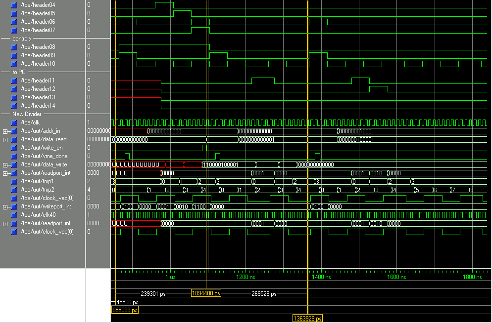
Three access cycles are shown, each starts after a yellow cursor line:
The mask register (address 0x8) is written (data 0x621).
The version register (address 0) is read and yields a 1
The mask register is read back and yields a 0x021, since the mask register is only 8 bits wide and the valid data are prepended with 0s.
Please note that the address actually sent on the header pins is 4 and it is multiplied by 2 to generate the VME address internally. The first nibble (LSB) of the data read out from the input FPGA are stable a short while after the 3rd clock transition of each access cycle. Due to the odd number of clock transitions per access cycle every other cycle starts on a falling clock edge !