ATLAS Level-1 Calorimeter Trigger
GOLD Module
-
V1.0-
Project Specification
Version 0.1
Date: 01/03/2011 16:52:24
Bruno, Eduard, Uli, Weina
Universität Mainz
1.2.3 Configuration,
monitoring, and control
1.2.3.1 Pre-configuration
access
1.2.3.3 Environmental
monitoring
3.4 Board
level issues : Power supplies and line impedances
3.5 Configuration
control and system monitor
Firmware, on-line software and tests
4 Interfaces
: connectors, pinouts, data formats
4.3 Backplane
connector layout
1
Introduction
This document describes the specification for the initial version 1.0 of the Generic Opto Link Demonstrator (GOLD). The specification covers the processor board as well as mezzanine modules carrying clock circuitry, controls, and opto-electrical receivers. Section 1 of this document gives an overview of the module. Section 2 describes the functional requirements. Section 3 details the implementation.
1.1 Related projects
The GOLD is a demonstrator for the Topological Processor, a major processor module within the future Cluster and Jet Processor scheme of the ATLAS level-1 calorimeter trigger. The Topological Processor will be located between the CMM++ and the CTP in the L1Calo architecture. A demonstrator for the CMM++ is the BLT. The future CTP is assumed to be electrically identical to its current incarnation, the firmware, and the data formats on the interfaces might be different.
TTC http://www.cern.ch/TTC/intro.html
L1Calo modules http://hepwww.rl.ac.uk/Atlas-L1/Modules/Modules.html
TTCDec http://hepwww.rl.ac.uk/Atlas-L1/Modules/Components.html
CTP http://atlas.web.cern.ch/Atlas/GROUPS/DAQTRIG/LEVEL1/ctpttc/L1CTP.html
CMM++ ???
1.2
GOLD
processor board
The Topological Processor within the L1Calo architecture is likely to be a single processor crate equipped with one or several processor modules. The processor modules will either be identical copies with firmware adapted to the specific topologies to operate on. Alternatively it could be modules tailored to a specific topology in hardware. The GOLD is a first technology demonstrator for the topological processor and other future L1Calo modules. These specifications describe its use as a Topological Processor demonstrator only. It is meant to be operated on output signals of a first prototype of the CMM++, or initially on the BLT.
The GOLD will receive the topological output data of the sliding windows processors. The details of the data formats are not currently defined. However, the information transmitted into the GOLD will be basically comprised of the ROI data that are currently transmitted to the 2nd level trigger. The data will consist of a description of the position of an object (jet, e/m cluster, and tau) along with some qualifying information, basically the energy sum within the object. Preliminary data formats have been devised. Data are going to be transmitted on optical fibres. After conversion to electrical representation, data are received and processed in FPGAs equipped with on-chip Multi-Gigabit Transceivers (MGT). Results are sent to the Central Trigger processor.
The GOLD will be designed in AdvancedTCA (ATCA) form factor. Together with its mezzanine modules, it will populate up to three adjacent slots of a standard ATCA shelf. Backplane connection, however, is made to a single ATCA slot only. The mezzanine modules make use of industry standard connector types, but they are built in GOLD specific PCB dimensions.
1.2.1
Real-time
data path
ATCA Backplane zones 2 and 3 of the GOLD are used for real-time data transmission. The module incorporates two distinct processing schemes. One is based on currently available FPGAs (XC6VLXT series); the other one tries to make use of FPGAs (XC6VHXT) meant to be available very soon. The baseline operation of the GOLD relies on the LXT scheme. The HXT FPGAs will not be mounted initially.
The CMM++ data enter the GOLD optically through the backplane. The fibres are fed via five blind-mate backplane connectors that can carry up to 72 fibres each. That limits the maximum aggregate bandwidth on the optical inputs to 3.6Tb line rate, if 10 Gb/s transmission is used throughout. Initially, however, the interfaces will be used at lower rates, and with just 12 fibres per connector. The optical signals are converted to electrical signals in 12-fibre receivers. Data reception is handled on a mezzanine module, stacked on the component side of the GOLD. The GOLD processor board is fed with electrical signals, which are routed through a total of four industry-standard FMC connectors with differential signal layout. Data from the two top most connectors are routed to four FPGAs, where they are de-serialised in MGT receivers; the parallel data are presented to the FPGA fabric. In the four input processors part of the algorithms are run, the actual topological algorithms requiring access to data from the full eta/phi space of L1Calo, however, are run on the main processor chip. The final results are transmitted towards the CTP on optical fibres. The signals are converted to electrical and de-serialised on an adapter module located near the CTP crate.
Both the implementation of the CTP link and the partitioning into input processors and main processor were chosen due to limitations on resources on currently available FPGAs only, and are not meant to reflect an architectural feature of a future Topological Processor.
The operation of the real-time data path requires low-jitter clocks throughout the system. For synchronous operation, data transmitters will have to be operated with clean multiples of the LHC bunch clock. Receiver reference clocks may as well be derived from local crystal oscillators, though tight limits on the frequency range will have to be observed. The GOLD module will be designed for 40.08 MHz operation of the real-time data path only.
Figure 1 shows a conceptual drawing of the GOLD (main components only). The processors are labelled A to D for the input processors, M for the main processor, E to H for the Virtex HXT sub-system. The mezzanine module connectors V to Y carry the optical input circuitry. Front panel connector zone and ATCA backplane connector zones Z1 to Z3 are indicated as well. More detailed diagrams are shown in section 3.
![]()
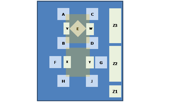
Figure 1: GOLD module
1.2.1.1 Input processing
The optical data arrive on the input mezzanine module on standard 12-fibre bundles. Since the backplane connectors support multiples of 12 fibres, the signals might in a future version of the board be supplied by “octopus” cable sets, splitting 24, 36, 48, or 72 fibres into groups of 12. It should be noted that un-armed, bare fibre bundles are very flexible and can easily be routed to their destination, even in high-density designs. However, they need to be protected from mechanical stress. The opto-electrical conversion will be performed in Avago or compatible 12-channel devices. Industry-standard SNAP12 devices are not considered an option, since so far no high-bandwidth SNAP12 devices are available from any supplier. The opto receivers chosen exhibit programmable pre-emphasis so as to allow for improvement on signal integrity for given track length.
As the number of electrical input channels may be higher than the number of optical inputs, the electrical signals are routed from the o/e converters into CML fan-outs, and then onto the mezzanine connectors. This will allow for evaluation of electrical duplication schemes that future algorithms will require. While the mezzanine module concept with a rather inexpensive and almost passive (except the fan-outs) carrier for the opto receivers is particularly useful in the demonstrator and prototyping phase, it is envisaged for future production modules as well. Such a concept allows for several instances of a topological processor to be run with different signal routing, optimised for the respective algorithms. The CML circuits do not allow for neither pre-emphasis nor signal equalisation. Therefore signal conditioning on the data sources and sinks is required, if longer tracks are to be used.
Once on the processor board, the multi-gigabit links are de-serialised in the input processor FPGAs. They allow for programmable signal equalization on their inputs. The exact data formats are as yet unknown, though standard 8b/10b encoding is envisaged for purpose of run length limitation and DC balance. The processors are supplied with required bias and termination voltages, as well as a suitable reference clock.
The input processors are assumed to do local pre-processing on the incoming data. The extent of local processing is determined by the respective algorithms.
1.2.1.2
Main
processor
The main processor has access to data from the full solid angle in eta and phi. Data volumes are limited by the general purpose I/O bandwidth of the FPGA. In the first iteration of the module a XC6VXLX240 is used. With a line rate of 1Gb/s and a total of 240 differential lanes into the main processor, the aggregate bandwidth is limited to 240 Gb/s. This theoretical limit cannot probably be reached, since a fraction of lanes might be required for control purposes, as the main processor dubs as a module controller. Bandwidth can be increased when larger, foot print compatible FPGAs are mounted on the PCB. The use of multi-Gigabit links on this path is not effective due to their higher latencies. 600-lane FPGAs of the XC6V series have been announced, but are not yet available. Due to the currently limited aggregate bandwidth of parallel I/O, the results of the topological algorithms are sent on to the Central Trigger Processor or other data sinks on multi-gigabit links. A single fibre-optical ribbon connection through the front panel of the module is provided for this purpose. An adapter board will be required to interface the GOLD to the LVDS inputs of the current CTP. This module will be equipped with CML-to-LVDS de-serialisers DS32EL0124 or similar. Additionally a small number of LVDS signals will be provided, so as to route latency critical signals directly to the CTP on electrical cables.
1.2.2 Clock distribution
Both the FPGA fabric and the multi-Gigabit transceivers (MGT) need to be supplied with clock signals of appropriate signal levels and signal quality. The fabric clocks are multiples of the LHC bunch clock at LVDS levels. The MGT clocks are CML level signals, AC-coupled into the MGT clock pads of the FPGAs. The jitter of the MGT clocks has to be tightly controlled. Clock generation and jitter clean-up are performed on a clock and control mezzanine module, located towards the bottom of the GOLD. The clock distribution trees are located on the GOLD processor board. The clock fan-out chips chosen are devices with multiple signal level input compatibility, and output levels suitable for their respective use, either LVDS or CML.
There are two independent clock trees for the fabric clocks into all FPGAs. There is one common MGT clock tree into all FPGAs. Another MGT clock tree supplies the main processor MGTs. There is yet another clock tree available to supply the high speed quads of the XC6VHXT devices (see below). The main processor receives additional local clocks since it handles DAQ, ROI, and control links as well.
1.2.3 Configuration, monitoring, and control
While the GOLD is basically meant to be a demonstrator for the Multi-Gigabit real-time data paths of future L1Calo modules, an attempt is made to prototype various module controls for future ATCA based modules as well.
1.2.3.1 Pre-configuration access
The GOLD is a purely FPGA-based ATCA module. There are no dedicated communications processors available on the module. Therefore there is only a single control path predefined that could possibly allow for access to a module with un-configured FPGA devices. This is the I2C port (IPMB) available on all ATCA modules in zone 1 (see below). Also CAN (see below) could be an option for pre-configuration access. Due to the very limited bitrates on these two networks, neither of them is considered suitable for initial access in a fairly experimental setup, where there is quite some probability for a flash card based FPGA configuration failing. FPGA configuration with up to the order of 100MB of configuration data per GOLD would be impossible to achieve through a service network of just hundreds of kilobits per second bandwidth.
For this reason the GOLD will be equipped with a USB microcontroller which supports 480Mb/s USB high-speed mode. The microcontroller is interfaced to the FPGAs via JTAG protocol. The microcontroller design is fully compatible to the Xilinx platform USB solution. Therefore the crucial operation of FPGA configuration is available from both Linux and Windows without the need for any software to be written. Either production firmware or service code can be loaded to the FPGAs, as required. Debug with the Xilinx Chipscope tool set will be supported out of the box. JTAG user access to the FPGAs will be possible with a sustained rate of several Megabits per second. However, some application software would need to be written for this purpose.
On the GOLD the USB sub-system will be built on a mezzanine module, though it is envisaged to make this pre-configuration and debug access port available as an integral part of future L1Calo ATCA production modules. Pre-configuration access beyond the use case described above would be possible, since the USB microcontroller can at any time be loaded with a non-Xilinx hex code via the USB. However, initially on the GOLD there will be no additional electrical connectivity available beyond the Xilinx standard wiring to the JTAG port. Hardware upgrade might be possible at a later stage, if required.
1.2.3.2 FPGA configuration
The baseline FPGA configuration scheme on the GOLD is via a CompactFlash card and the Xilinx System ACE chip. This configuration scheme has been successfully employed on several L1Calo modules so far, including the JEM. On the JEM the required software and firmware has been devised to allow for in-situ update of the CompactFlash images. The required board-level connectivity will be available on the GOLD, to write the flash cards through some network connection to the FPGAs, once they are configured. The inevitable bootstrap problem is solved through the USB based pre-configuration access scheme described above.
1.2.3.3 Environmental monitoring
Board level temperature and voltage monitoring will be a requirement on future L1Calo modules. The current L1Calo modules are monitored via CAN bus. The default ATCA monitoring and control path is via I2C links in zone 1. For the GOLD both monitoring paths will be available. The backplane I2C link (IPMB-A only) is run via an IPMB compatible driver into the control CPLD. This CPLD is basically used for a further stage of routing only. The I2C controller can be located either in the main processor FPGA or inside a microcontroller located on a mezzanine module on the GOLD. It will be possible to mount a CAN microcontroller on a future version of the clock/control mezzanine. The required connectivity is available on the mezzanine socket. Initially an FPGA based state machine will handle the I2C connection. On the GOLD only configured FPGAs can be monitored for die temperature and internal supply voltage. This is achieved by the use of their built-in system monitor. On future modules these measurements might be complemented by board-level monitoring points.
1.2.3.4 Module control
On standard ATCA modules, IP connectivity is mandatory for module control. This is generally provided by two 10/100/1000 Ethernet ports on the backplane in zone 2 (redundant base interface). This is a requirement for an ATCA compliant backplane, but not for an ATCA compliant module. The module is free to ignore the Ethernet ports and provide IP connectivity by any suitable means. On a future L1Calo ATCA crate one would probably avoid wiring two slots exclusively to the two base interface ports. On the GOLD a few differential signal pairs towards the bottom of the module are reserved for module access via Ethernet, PCIe, or other connectivity. The respective lines are wired to the clock/control mezzanine, where the required connectivity can be made to a local microcontroller, an SGMII Phy device, or straight into an MGT link on the main processor. A dedicated SFP based control link into the main processor will transport module control signals initially. It will be connected into an optical VME bus extender, so as to allow controlling the GOLD from a VME crate CPU within the current L1Calo online empire.
1.2.3.5 DAQ and ROI
Since the GOLD would be used in the existent phase-0 environment initially, a scheme for transmitting event data into the ATLAS data acquisition and 2nd level trigger was made compatible to the existent modules. A single optical channel into each the DAQ and ROI RODs is provided on the clock mezzanine module. The optical interface is made via SFP sockets. Since it is not yet known whether it will be necessary and possible to implement the G-Link protocol on Xilinx MGT circuits, the SFPs can alternatively be driven from the FPGA fabric, if a new clock mezzanine module is made. There are enough resources available on the clock mezzanine socket to allow for either MGT or fabric based connectivity into DAQ and 2nd level trigger.
1.3 Opto module
The opto module is a mezzanine module on the GOLD processor board. It is stacked on the component side of the GOLD with four FMC standard connectors. All FMC connectors are of same signal type specific pin allocation. Thus four identical mezzanine modules can be mounted on the GOLD, though for reason of module mechanics and keep-out zones on the processor board, a mezzanine module would normally be connected via two or four FMC connectors for a half-size, or full-size mezzanine board respectively. A four-connector mezzanine module will require special tools so as to be removed from its sockets, for reason of retention forces.
As outlined above, the baseline opto module will carry five fibre-optical backplane connectors. Initially Molex MTP-CPI connectors are used. Sockets for up to six 12-channel opto devices will mechanically fit a half-size mezzanine module. The first opto module to be manufactured will be aimed at link tests, not requiring external data sources. It will therefore be populated with two optical transmitters and three optical receivers. The electrical MGT signals will be routed such that receive and transmit lines will end up properly paired in the respective MGT quads of the FPGAs. This will allow for automated MGT signal integrity scans with help of the Xilinx IBERT tool.
At a later stage opto modules with higher input link counts and higher optical fibre densities will be built, targeted at setups for system level tests with CMM++ modules.
For reason of opto device availability, initial versions of the opto module will be based on the Avago transceiver chip set. The module might be re-designed for different devices (SNAP12) if high-speed versions were to appear on the market.
Also the envisaged electrical signal duplication, initially implemented with Micrel CML fanout chips might be reworked in a further iteration of the module, if a test bench for crossbar switches were required.
1.4 Clock/control module
Clock reception and conditioning circuitry is implemented on a mezzanine board. The mezzanine connector carries all required clock signals (multiple MGT and fabric clocks for the FPGAs), as well as general control signals. Due to the limited real estate of the clock mezzanine more than one version of the clock module will be built so as to try out a variety of possible clock schemes.
The current L1Calo modules receive their LHC bunch clock and associated data through the TTCDec module, based on a TTCRx chip. This is not assumed to be the way TTC data and clocks are going to be distributed in a future L1Calo architecture. The GOLD will have to operate with the existent clock distribution scheme initially. At a later stage it will probably be driven in a different way. For backward compatibility it is assumed that a TTCDec module will be connected to the GOLD. Due to lack of space this will be interfaced to the clock module through an external connection on the front panel. Just a very small number of single ended TTC data signals are actually used on the current L1Calo modules. For the TTCDec interface it will therefore be assumed that an external TTCDec module is interfaced to a CPLD locally. That will allow for a programmable selection of TTC data, as well as for personalisation of the TTCrx chip at power-up. The selected data will be transmitted as source terminated or slew rate limited single-ended CMOS data into the GOLD. A low data rate I2C port will be available for TTCRx configuration. The LHC bunch clock will run on a differential signal pair for reason of signal integrity.
Alternatively optical data transmission of clock signals onto the clock mezzanine module will be possible. The DAQ and ROI SFP modules described above are used for data transmission only. The two corresponding optical receivers are available to route LHC clock and data into the GOLD.
On an initial version of the clock module there will be a jitter reduction scheme in operation, based on the National Semiconductors LMK03000 chip. This will be required for reason of signal integrity, when operating MGT links with the jitter prone TTCDec recovered clock. This circuit might not be required when using an optically distributed clock signal. In this case centralised jitter elimination at the optical clock source might be sufficient.
1.5 HXT processor
The GOLD, as described above, is the module version that will be assembled initially. It makes use of FPGA processors that are available on the market currently. The five FPGAs of type XC6VLXT are mounted in the top half of the GOLD, with their MGT inputs connected to the top pair of FMC connectors. They cover about a third of the real estate of the module. Another third is taken by auxiliary circuitry and connectors. This leaves a third of module space for another four FPGAs of type XC6VHXT. Those FPGAs should appear on the market rather soon. They provide higher MGT link counts and speeds, as well as higher processor capacities. HXT processors might be used on future L1Calo modules, though the properties of the MGT circuitry compare rather unfavourable to the next coming Virtex-7 family. The HXT devices suffer from a split bitrate range of up to 6.5 Gb/s for the slower MGTs, and a non-overlapping 10Gb/s only for the faster transceivers on the same chip. That is very inconvenient and it imposes considerable limitations on an architecture based on such devices.
The GOLD allows for mounting one pair of HXT devices connected to the lower pair of FMC connectors. Another pair of these FPGAs is wired to zone 2 of the ATCA backplane connector. The HXT subsystem is not within the scope of this specifications document, however, there will be an appendix added to a future version of this document giving a few details on the HXT design. It should be noted that the power distribution system of the GOLD was designed to allow for concurrent operation of the LXT and the HXT subsystems. However, dissipation of the module would require special consideration when operating all of the FPGAs at full performance concurrently.
2 Functional requirements
This section describes the functional requirements only. Specific rules need to be followed with respect to PCB design, component placement and decoupling. These requirements are detailed in section 3. For information on interfaces with other system components, see section 4. Requirements for the Virtex-6 HXT subsystem are listed separately.
2.1 Signal paths
The GOLD is designed for high speed differential signal transmission, both on external and internal interfaces. Two differential signalling standards are employed: LVDS and CML. There is a very small amount of single ended connectivity required on the GOLD. This section covers basic signalling requirements only; there is a separate section on signal integrity in sect. 3.3.
The requirements with respect to signal routing are:
- Route all differential signals at 100 Ω differential track impedance
- Use internally sink-terminated devices throughout. Any non-terminated high-speed devices need to be documented in a separate list.
- Use LVDS signalling on all connections into the FPGA fabric, for both data and clocks
- Design all LVDS interconnect for 1Gb/s signalling rate
- Use DC coupling on all LVDS lines
- Use CML signalling on all MGT lines, for both data and clocks
- Design all MGT data links for 10Gb/s signalling rate
- Use AC coupling on all MGT differential inputs and outputs, for both data and clocks
- Use CML on all common clock trees; rather than using AC coupling, observe the signalling voltage and input compatibility rules as outlined by the device manufacturers
- Use source terminated single ended CMOS signalling for JTAG and configuration lines, where required. Avoid impedance discontinuities on clock lines.
- Observe the requirements on overshoot and undershoot limitation, in particular for System ACE and FPGA JTAG and configuration lines. Use slew rate limited signals.
2.2 Real-time data reception
Real-time data are received optically from the back of the ATCA shelf; they are converted to electrical representation, and fanned out on a mezzanine module. They are transmitted to the processor board and de-serialised and processed on the input processor FPGAs. The use of a mezzanine module is a requirement, since choice of alternative opto receivers and algorithm-specific routing should be possible at low NRE cost.
The requirements with respect to the opto mezzanine are:
- Provide four FMC connectors on the GOLD for connection of the opto transceivers to the input processor FPGAs
- Use identical pinout on all FMC connectors to allow for variable size mezzanine modules
- Provide 72 differential input links
- Provide 12 differential output links for test purposes
-
Provide 13 single-ended 3.3V CMOS control lines (incl.
I2C and JTAG),
power 2V5/3V3, ground
- Use XILINX ML605 FMC pinout for reference
- Deal with any required input signal conditioning at mezzanine level:
- Duplication
- AC coupling
The requirements with respect to data reception and conditioning are:
- Provide five MPO/MTP compatible blind-mate fibre-optical backplane connectors in ATCA zone 3
- Route bare fibre bundles to 12-channel opto receivers
- Allow for up to 3 standard sized opto receivers per FMC connector (i.e. total of 12 on a full-size mezzanine module)
- Fan out CML level electrical signals
- Supply optical and electrical components with appropriately conditioned supply voltages
- Provide suitable coupling capacitors
- Run the signal paths into the input processors
- Allow for footprint compatible medium- and high-end FPGAs with up to 36 MGT links per chip
2.3 Real-time data processing
The GOLD processing resources are partitioned into four input processors and a main processor. This is not a requirement, but a consequence of limitations on MGT link count and processing resources on currently available FPGAs. The requirements on processing resources depend on the physics algorithms and are not currently known.
The requirements with respect to the processors are:
- Provide an aggregate input bandwidth of 92 GB/s (payload) into the processors
- 144 channels of up to 6.4Gb/s line rate
- Process the real-time data in a 2-stage (maximum) processing scheme (input and main processor)
- Minimise latency on chip-to-chip data transmission
- Maximise bandwidth between the two processing stages
- Send output data to CTP on MGT links, so as to maximise low-latency inter-processor communication bandwidth
- Use higher latency channels for non-RTDP links where possible
- Use CPLDs as “port expanders” for low-speed signals
- Use spare resources on the main processor for board level control functionality
- Provide an aggregate bandwidth of up to 8 GB/s (payload) on MGT outputs towards the CTP
- 12 channels of up to 6.4Gb/s line rate
- Additional 12-channel low latency electrical (LVDS) port
2.4 Clock distribution
Both the FPGA fabric and the MGT links need to be supplied with suitable clock signals. Due to the synchronous, pipelined processing scheme most of the clocks need to be derived from the LHC bunch clock or a device emulating it. Due to requirements on MGT reference clock frequency accuracy, a mixed 40.00/40.08 MHz operation is impossible. Therefore a requirement for 40.08 MHz operation has to be introduced.
Some clocks are generated on the clock mezzanine module. They are fanned out to the sink devices with active components located on the main board. General requirements on signal routing and signal integrity are outlined elsewhere.
The requirements with respect to the clock distribution on the main board are:
- Provide the FPGAs with clocks of multiples of either a 40.08MHz crystal clock, or the LHC bunch clock
- Provide a common MGT clock to all FPGAs.
- Provide a second MGT clock to the main processor
- Provide a separate MGT clock to all HXT FPGA devices
- Connect the MGT clocks to the LXT FPGAs such that the central quad of 3 quads is supplied. This rule must be followed such that the requirements are met, whether the smaller or the larger device is mounted.
- Provide two common fabric clocks to all FPGAs
- Provide a separate crystal based MGT clock to the main processor for use on the control link
- Provide a separate crystal based MGT clock to the main processor for use on the DAQ and ROI link outputs (40.00 MHz or multiple)
- Provide a separate crystal based 40.08 MHz (or multiple) MGT receive reference clock to the main processor on the receive section of the DAQ and ROI links, for use on future LHC bunch clock recovery circuitry (TTCDec replacement), and thus:
- Allow for the input portion of the DAQ and ROI transceivers to be used for optical reception of LHC clock and data
The requirements with respect to the clock generation on the mezzanine board are:
- Receive a TTC signal from backplane zone 2
- Receive a TTC bunch clock through an external connection to a TTCDec module, at LVDS signalling standards
- Provide for single ended connectivity to the TTCDec to receive TTC data (broadcasts, counter resets) and control the TTCRx chip via I2C
- Allow for insertion of clock conditioning hardware into the clock path
- Provide for a fall-back to a 40.08MHz (or multiple) crystal reference
The clock mezzanine module provides some connectivity and real estate for general control purposes. The requirements with respect to auxiliary controls on the clock mezzanine board are:
- Receive a CAN signal from backplane zone 2
- Receive a single USB signal pair from backplane zone 2
- Route the USB signal on to the JTAG mezzanine, if it isn’t handled on the clock mezzanine
- Receive a 4-pair Ethernet signal from backplane zone 2
- Connect the clock mezzanine to the main processor via a single MGT for purpose of module control
- Connect the clock mezzanine to the main processor via 12 LVDS pairs
- Communicate to the control CPLD on the main board
2.5 Configuration and JTAG
JTAG is used for board level connectivity tests, pre-configuration access, and module configuration. During initial board tests and later hardware failure analysis, JTAG access will be required to connect an automatic boundary scan system, generally when the module is on a bench, not in an ATCA shelf. Also the initial configuration of non-volatile CPLDs will be performed at that stage.
The requirements with respect to boundary scan and CPLD configuration are:
- Allow for the connection of a boundary scan system to all scannable components of the GOLD: FPGAs, CPLDs, System ACE, and mezzanine modules via standard JTAG headers, following the standard rules on pull-up, series termination, and level translation between supply voltage domains.
- Allow for CPLD (re)configuration, following the boundary scan tests, and occasionally on the completed system.
- There is currently no requirement known regarding integration of devices sourcing or sinking MGT signals externally, into the boundary scan scheme
Pre-configuration access and device configuration of the FPGAs is required at any time. USB access and the System ACE / CompactFlash configuration scheme are employed.
The requirements with respect to USB access and FPGA configuration are:
- Employ the standard System ACE configuration scheme to configure the FPGAs upon power-up
- Connect the System ACE external JTAG port into an USB-to-JTAG converter according to Xilinx ML605 configuration scheme
- Connect the USB processor to a front panel mini USB socket
- Alternatively connect the USB (data lines only) via the clock/control mezzanine module to the zone2 backplane connector
- Allow for static control of the FPGA configuration port settings and read-back of the status via the control CPLD.
2.6 Module control
On ATCA modules serial protocols are used to achieve board level configuration and control. Typically Ethernet would be used to control module operation. On the GOLD any serial protocol compatible to Xilinx MGT devices can be used to communicate to the main processor, once it has been configured. Examples are SGMII / Ethernet, PCI-Express, or any application specific protocol. All board level control goes via the main processor.
The requirements with respect to general board control are:
- Provide an optical bidirectional channel from the front panel to a the main processor MGT (control link)
- Provide four-lane access from zone 2 to the clock/control mezzanine, compatible to 10/100/1000 Ethernet, so as to allow for a Ethernet Phy to be mounted on the mezzanine module
- Provide two-lane access from the mezzanine on to the main processor (one MGT, bidirectional)
- Provide bi-directional connectivity between input processors and main processor via a subset of the general routing resources otherwise used for the real-time data path
- Provide unidirectional transmission from each input processor to the main processor via four MGT lanes for additional monitoring bandwidth
- Provide a 12-wide single-ended 2.5V-CMOS bus between main processor and control CPLD
- Have the CPLD act as a port expander for low-speed and static control
The CPLD is in charge of mainly static controls and low speed I2C fanout.
The requirements with respect to the CPLD are:
- Communicate to the general board control system via a 12-wide bus to the main processor.
- Communicate to the opto transceivers located on the mezzanine module, via I2C and static lines
- Communicate to the on-board optical transceivers (12-channel Avago and SFP)
- Communicate to any CPLD located on the clock mezzanine module
- Communicate to the IPMB-A port via I2C protocol
- Communicate to the System ACE sub-system so as to control FPGA configuration and allow for in-situ update of the CompactFlash card
- Control the static FPGA configuration control lines
2.7 DAQ and ROI
A single fibre for each DAQ and ROI transmission will be provided on the GOLD.
The requirements with respect to DAQ and ROI interface are:
- Provide an optical ROI output channel to the front panel
- Provide an optical DAQ output channel to the front panel
- Use standard SFP modules
- Allow for wiring to either MGT or fabric resources of the main processor via the clock/control mezzanine module
- Provide a separate 40 MHz (or multiple) clock to the MGT quads driving DAQ and ROI fibres
3 Implementation
This section describes the detailed implementation of the module and it specifies a set of design rules needed to comply with general signal integrity rules, as well as component specific requirements.
The GOLD is built as an up to 3 slots wide ATCA module, so as to accommodate thick components on the bottom of the module, and mezzanine modules on the top. The module carries processors from two FPGA families, XC6VLX and XC6VHX. The latter will not be mounted initially.
The main board is built as a 16 layer PCB. The PCB is approximately 2mm thick and should fit ATCA standard rails. If required, the board edges would be milled down to the required thickness. A detailed block diagram of the real-time data path is shown in
Figure 2.
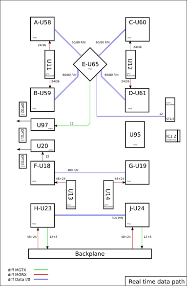
Figure 2 – GOLD real-time data path
3.1
Scalable
design
The GOLD can be assembled with either
XC6VLX240T or XC6VLX550T devices, so as to allow for both affordable and
maximum-bandwidth components. GOLD needs to be designed such that all vital
signals of both MGT and general I/O type are run on signal pins available on
the smaller device. Since GOLD is a rather experimental setup, component
placement should be chosen such that incremental component assembly and re-work
are simplified, where possible.
The mezzanine module sockets need to provide spare connectivity to
make sure that GOLD functionality can be upgraded at a later stage by replacing
the relatively inexpensive mezzanine modules only.
3.2
Clock
The clock distribution is spread over a clock mezzanine module, for clock generation, and the GOLD main board, for fan-out. Various Micrel device types are used to drive and fan out clocks of LVDS and CML type at low distortion. All Micrel devices are sink terminated on-chip. A detailed block diagram of the clock path is shown in Figure 4.
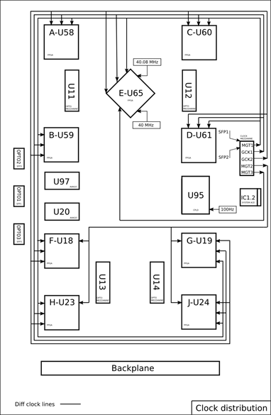
Figure 3 – GOLD clock distribution
3.3
Control
A detailed block diagram of control paths is shown in Figure 4.
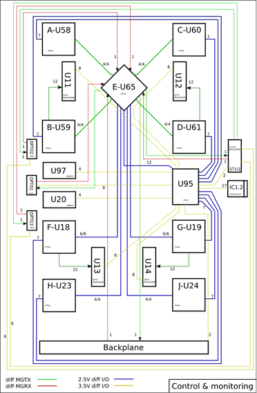
Figure 4 – GOLD control paths
3.3.1 Module control
GOLD module control is initially done via a serially extended VME bus, as outlined above. This choice was made since such an operation will not require any access-mode specific online software to be written. The module is seen from a VME crate CPU as if it were a local VME module.
As soon as the required software environment is available, this access mode will be converted to standard Ethernet access. The required hardware components are available on the GOLD: The optical (SFP) link can be directly connected to any 1000BASE‑SX Ethernet port. Also, there is the required space and connectivity available on the clock/control mezzanine to connect the main processor to the electrical Ethernet port located on the backplane, via an SGMII Phy (M88E1111 or similar).
While the existent BLT demonstrator module is currently equipped with a standard VME – – interface, it is envisaged to retrofit the BLT with additional Ethernet circuitry. VME access would such be shadowed by Ethernet-based control. That would allow for more realistic tests of the Ethernet control scheme with more than one module.
The use of Ethernet for module control has been extensively explored in a previous project. Both UDP[1] and bare Ethernet schemes have been used. Reference implementations (hardware/firmware/software) are available.
Warning -- the electrical Ethernet on the GOLD will not be compliant with the ATCA base interface, unless backplane pin-out is chosen appropriately. The required documentation is not available to the GOLD module designers!
3.4 Board level issues : Power supplies and line
impedances
The GOLD is a large, high-density module, carrying large
numbers of high-speed signal lines of various signal levels. The module relies
on single ended CMOS (2.5 and 3.3V), and differential (some or all of LVDS,
PECL3.3, PECL2.5, CML3.3, CML2.5) signalling. System noise and signal integrity
are crucial factors for successful operation of the module. Noise on operating
voltages has to be tightly controlled. To that end, large numbers of decoupling
capacitors are required near all active components. FPGAs are particularly
prone to generating noise on the supply lines. Their internal SERDES circuitry
is highly susceptible to noisy operating voltages, which tend to corrupt their
high-speed input signals and compromise the operation of the on-chip PLL,
resulting in increased bit error rates. To suppress all spectral components of
the supply noise, a combination of distributed capacitance (power planes) and
discrete capacitors in the range of nF
to hundreds of mF
are required. On the FPGAs there are capacitors included in the packages for
decoupling of noise up to highest frequencies.
The GOLD base frequency is 40.08 MHz. Parallel differential I/O operates at multiples up to 1Gb/s. Multi-Gigabit (MGT) links operate at 6.5 or 10Gb/s Those signals are routed over long tracks on-board and across the backplane. This is only possible on matched-impedance lines. Differential sink termination is used throughout. All FPGA inputs are internally terminated to 100Ω or to 50Ω||50Ω, according to the manufacturer’s guidelines. All lines carrying clock signals must be treated with particular care.
The rules with respect to signal integrity are:
·
Use low-noise local step-down regulators on the
module, placed far from susceptible components.
·
Observe power ramp and sequence requirements for
FPGAs
·
Run all supply voltages on power planes, facing
a ground plane where possible, to provide sufficient distributed capacitance
·
Provide at least one local decoupling capacitor
for each active component
·
For FPGAs, follow the manufacturer’s guidelines
on staged decoupling capacitors (low ESR) in a range of nF
to mF
·
Observe the capacitance limitations imposed by
the voltage convertors
·
Minimise the number of different VCCO
voltages per FPGA to avoid fragmentation of power planes
·
avoid large numbers of vias
perforating power and ground planes near critical components
·
avoid impedance discontinuities on single ended
clock lines
·
source-terminate single ended clocks with
approximate impedance
·
Route all differential signals on properly
terminated, controlled-impedance lines:
o Have all micro strip lines face a ground plane
o Have all strip lines face two ground planes or one ground plane and one non-segmented power plane
o
avoid sharply bending signal tracks
o minimise cross talk by running buses as widely spread as possible
o Avoid in-pair skew, in particular for MGT links and clocks
o Avoid impedance discontinuities and stubs, in particular on MGT links and clocks
o
Use LVDS on all general-purpose FPGA-FPGA links
o
Use LVDS on all GCK clock lines
o
Use PECL or CML on all MGT clock lines
o
Use CML on all MGT data lines
o
Use AC coupling on all MGT clock inputs
o
Use AC coupling on all MGT data inputs
o
For all off-board links assume capacitors
off-board
o
For on-board links place capacitors close to
source
o
Use AC coupling when crossing PECL/CML domains
o
Use AC coupling or suitable receivers when
crossing 2.5V/3.3V domains, except on LVDS
o
Use bias networks on AC coupled inputs where
required
o
Run FPGA configuration and FPGA JTAG clock lines
on approximately 50 W
point-to-point source terminated lines
According to the device specifications the following supply
voltages need to be applied to the FPGAs: Vccint=1.0+/-0.05V,
Vccaux=2.5V. All bank voltages are chosen to be 2.5V.
On all voltages observe the device specific ramp up requirement of 0.2ms to
50ms.
On GOLD most of the FPGA based board level I/O is done via LVDS
signalling. Some rules should be followed so as to efficiently exploit these
resources.
The rules with respect to general I/O connectivity are:
·
Tie Vccaux and all
bank supplies to 2.5V. A given FPGA is supplied by only one 2.5 V plane.
·
Use all FPGA banks for LVDS and low-current,
point-to-point 2V5 CMOS only
·
On any external single ended links that might
generate ringing at the FPGA inputs, use series resistors or slew-rate limited,
or low-current outputs
·
No reference voltages nor DCI termination are
required for single ended general I/O. Use respective dual-use pins for I/O
purposes
3.5
Configuration
control and system monitor
Some single use and dual use pins are dedicated to control pre-configuration and configuration behaviour. Some pins are tied to appropriate logic levels via resistors; others are wired to CPLD outputs.
The rules with respect to pre-configuration and configuration control pins are:
·
The VFS pin is the fuse programming supply
voltage. Allow for wiring to GND (0Ω) or external 2.5V supply. Wire to
GND.
·
Allow HSWAPEN to be jumpered
to either Vcc or GND
·
Allow mode lines M0, M2 to be jumpered to either Vcc or GND.
Pre-wire to Vcc
·
Connect M1 to the CPLD (GND=JTAG mode, Vcc=slave serial)
·
Connect PROGRAM, INIT and DONE lines to the CPLD
·
Pullup DONE 330Ω,
INIT 4k7 PROGRAM 4k7
·
Connect Vbatt to GND
·
Wire DIN, DOUT and CCLK (series terminated)
configuration lines to the CPLD
·
Allow for wiring RDWR and CSI to either Vcco or GND
The rules with respect to system monitor pins are:
·
Do not use temperature sense lines DXN,DXP and
short them to GND
·
Decouple analog power
and GND according to UG370 with ferrite beads and wire the system monitor for
internal reference (both Vref pins to analog GND)
·
Do not use analog
sense lines Vn and Vp and
connect to analog GND
Firmware, on-line software and tests
The GOLD is an entirely FPGA based module. For both hardware commissioning and operation a set of matching firmware and software will be required. These two phases are well separated and requirements differ considerably. Hardware debug and commissioning will require intimate knowledge of the hardware components and will therefore be in the hands of the hardware designers. Both firmware and software will be restricted to simple, non-OO code. Hardware language is VHDL, software is plain C. GUI based tools are not required and will not be supplied by the hardware designers. Module commissioning from a hardware perspective is considered complete once the external hardware interfaces, board level connectivity, and basic operation of the hardware devices have been verified. The hardware debug and commissioning will involve JTAG/boundary scan, IBERT/ChipScope tests, and firmware/software controlled playback/spy tests with any data source/sink device available. Initially the BLT will be available for test vector playback on a single 12-fibre port. A debug opto module for the GOLD will be built with both fibre receivers and transmitters. At a later stage a CMM++ prototype module will be used as a data source.
Module control is initially via an opto fibre connection to a 6U VME-bus module carrying SerDes devices and optical transceivers. The opto-electrical interface will be a SFP module with LC-type opto connectors. Control software will be based upon calls to the CERN VME library. SFP outputs provided for DAQ and ROI data transmission will be tested for bit errors and link stability only. No specific data formats will be tested on these links.
In parallel to the hardware debug and commissioning, higher level software and firmware will be developed for later operation of the GOLD. As yet no decisions on languages and architecture have been taken. As far as control software is concerned, a board level control scheme for future L1Calo modules needs to be devised. This will most likely not follow the initial approach of VME serialisation.
The test environment available in the home lab will allow for simple real-time data path tests only. There is no hardware, software installation, nor expertise available to run any tests involving DAQ/RODs/ROSes. Therefore all system level tests will have to be done in an appropriately equipped L1Calo test lab. Currently the CERN test rig seems to be the only available option.
There will be a separate document on software and on algorithmic firmware produced at a later date.
4 Interfaces : connectors, pinouts, data formats
4.1 Internal interfaces
The opto mezzanine module is connected via up to four FMC style connectors (Samtec SEAM on the mezzanine module, SEAF on the GOLD) of identical pinout:
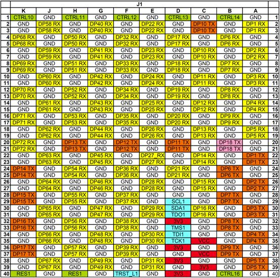
Figure 5: FMC pinout, connector J1 shown
The clock mezzanine module is connected via a xx-pin connector (Samtec SEAM series)
4.2 Front panel
The front panel shows the CompactFlash card for System ACE configuration, an electrical connector (LVDS) for CTP interconnect, and five optical connections: One MPO/MTP connector each for the real-time output to the CTP adapter from the LXT and HXT sub-system, and an SFP opto module to each DAQ, ROI and VMEbus extender. Further: a mini USB connector for FPGA configuration, and JTAG sockets.
4.3 Backplane connector layout
The backplane connector is made to standard ATCA layout in zones 1 and 2. Zone 3 is populated with five MTP/MPO connectors that connect onto a RTM with hermaphroditic blind-mate shrouds (MTP-CPI).
5 Appendix
5.1 Glossary
|
1000BASE‑SX |
Ethernet optical (multimode) physical layer |
|
8b/10b |
Industry standard data encoding scheme for purpose of DC balance and run length limitation (bit change enforcement) |
|
ATCA |
Advanced TCA, Advanced Telecommunications Computing Architecture |
|
Avago |
Manufacturer of 12-channel opto-electrical transceivers. The Avago transceivers used on the GOLD are not SNAP12 compliant! |
|
Base interface |
ATCA compliant backplanes provide pre-defined redundant IP connectivity via Ethernet 10/100/1000 from each slot to two modules in the crate (dual star) |
|
BLT |
Backplane And Link Tester module, fits in CMM slot of the L1Calo processor backplane |
|
CAN |
Controller Area Network, a differential serial bus (automotive) |
|
CML |
Current Mode Logic, a high-speed differential signalling standard |
|
CMM++ |
Future replacement of the L1Calo Common Merger Module |
|
CTP |
The Central Trigger Processor of ATLAS |
|
DAQ |
Data Acquisition (link). Physical layer G-link compatible |
|
FMC |
FPGA Mezzanine Card, as defined in VITA-57. Connector types Samtec SEAF/SEAM or compatible |
|
G-link |
Pre-historic HP/Agilent Phy chip. ~ 1Gb/s, proprietary link encoding scheme |
|
GOLD |
Generic Opto Link Demonstrator |
|
HXT |
Virtex-6 high end device type, equipped with two types of MGTs: low-speed MGTs with up to 6.5Gb/s line rate, high speed MGTs with 10Gb/s only. |
|
IBERT |
Xilinx automated bit error rate test tool for MGTs |
|
IPMB |
Intelligent Platform Management Bus (redundant, IPMB-A and IPMB-B), located in ATCA zone 1 |
|
LVDS |
Low-Voltage Differential Signalling standard |
|
LXT |
Initially available device type within Virtex-6 product range. Supports up to 6.5 Gb/s line rate on MGTs |
|
MGT |
Multi-Gigabit Transceiver |
|
MPO/MTP |
Industry standard optical connector for fibre bundles, here 12-72 fibres |
|
Phy |
A device implementing the physical level (electrical representation) of a network protocol |
|
Quad |
The Virtex-6 Serialiser/Deserialiser circuits are arranged in tiles of four MGT links each |
|
ROI |
Region of Interest, as signalled to 2nd level trigger. ROI link to Level-2 has G-link data format |
|
RTDP |
Real-time data path, i.e. the data path going to the CTP. Latency critical path. |
|
RTM |
Rear Transition Module (note: ATCA RTMs mate with the front modules directly in Zone 3, not via the backplane) |
|
SGMII |
Serial Gigabit Media Independent Interface (for Ethernet Phy), 1.25Gb/s |
|
SNAP12 |
Standard defining the electrical interface of opto-electrical transceivers |
|
TTCDec |
L1Calo specific mezzanine module for connection to the ATLAS Timing, Trigger and Control system, based on the TTCrx chip |
|
VME(bus) |
Versa Module Eurocard (bus). The GOLD is optionally connected to a VME module for purpose of module control, via a bidirectional serial link, due to lack of an ATCA shelf computer. |
|
Zone |
ATCA connector zones 1 (mainly power), 2 (backplane data links), 3 (RTM connections) |
5.2 Change log
2011
Jan 18 – added drawings
Jan 19 – corrected drawings
Jan 25 – updates of drawings and sect. 3.3.1