This is a collection of ideas for the
GOLD module. This is meant to be converted into proper specs ASAP. The format
of the final document is meant to be set by the JEM specs, from which a
skeleton in the src directory is to be derived. This
is a document under construction. Please check back regularly.
Overview:
The GOLD is meant to be a demonstrator for the
Topological Processor, a major component of the L1Calo Trigger. The GOLD is built
to receive up to a total of 288 multi-Gigabit links (from a set of CMM++s) and
feed them into processor FPGAs. After internal de-serialisation data are
processed, and a very small volume of data is sent to the output devices
(towards the CTP).
The Gold is of ATCA form factor. It is a double
(triple?) width
module due to the fact that it carries daughter modules. On the bottom of the
board there are components that exceed the acceptable height and therefore
require an empty slot with a modified front panel to the left of the GOLD. The
GOLD carries 8 processor chips and a merger. The latter doubles as a board
level controller.
External connectivity:
Connectivity is designed for the intended use of the
module: Many inputs from the back of the module, few optical outputs on the
front panel. A small number of outputs from a subset of the FPGAs is routed to the backplane. All backplane and front panel
I/O is via multi-Gb serial links, differential, 100Ω.
Opto-electrical conversion of the external signals is performed mainly on
daughter modules and in adjacent slots of the ATCA backplane.
Board level connectivity:
Most board level local routing is differential, 100Ω, using
FPGA parallel I/O. Single ended I/O is restricted to I2C control. No impedance
is specified for those lines. Spare mGb outputs on
the (which?) processor chips and spare mGb inputs on
the merger are available as additional non latency optimised resource.
The backplane use is to ATCA standards: power and
environmental monitoring in zone 1, module control (to merger?!?) and backplane
user I/O in zone 2, and connectivity to a rear transition module in zone 3.
Electrical connectivity in zone 2 is differential, DC
coupled (??). If required, AC coupling must be implemented on the remote
modules.
The GOLD is comprised of 3 banks of FPGAs. There is a
high level of connectivity within these 3 banks. Connectivity between the 3
banks is very low and is to be used for module control only. The 3 banks of
FPGAs are conceptually different:
There is one bank of 5 FPGAs of LXT type located
towards the top of the module. The footprint allows for two different devices
to be mounted: XC6VLX240T or XC6VLX550T in FF1759 package. Four of the FPGAs
act as processors. They carry external mGb inputs
only (except xx lines for debug). The 5th FPGA is wired to serve as
a merger for results from the processor FPGAs. The merger FPGA also takes the
role of a module controller. The
processor FPGA mGb input lines (total of 144 pairs)
are DC coupled to a pair of daughter module connectors of standard FMC-HPC pin
out. The connector carries differential signal lines and a small number of
control lines (I2C, 3.3V). Spare connector pins are connected to power, mGb outputs (mainly for debug purpose) and extended,
differential daughter module control. Please note that due the different
connectivity of LX240 vs. LX550 it needs to be checked that a sufficient and
symmetric level of connectivity is retained when the LX240 is used ! (needs discussion). In the
drawing the numbers of signal pairs are shown as x/y, where x is the signal
count for LX240, y is the signal count for LX550.
The second and the 3rd bank are designed for
two HXT type FPGAs each. The FF1924 footprint supports both XC6VHX380T and
XC6VHX565T. RTDP board level connectivity is available only within a bank of
two chips. The 2nd bank mGb I/O is wired
to a pair of FMC-HPC connectors as described above. The 3rd banks mGb I/O is wired to ATCA zone 2. The details of board level
and I/O connectivity are found in Table x. At current we assume that board
level connectivity is the same for both members of the HXT family chosen (to be
checked). In the drawing we distinguish 6.5 Gb/s (low)
lines from 10Gb/s (high speed) lines with the notation low+high.
Please note that some of the shown control circuitry
shown might currently not be implemented. Some time ago we discussed about a
control daughter, where some more control could reside. I believe that we are
currently planning for a clock daughter only. Not sure whether real-estate and pin-out
allow for control functionality!
We need to add a more detailed drawing for clock trees
and special control (I2C, system monitor ?? …)
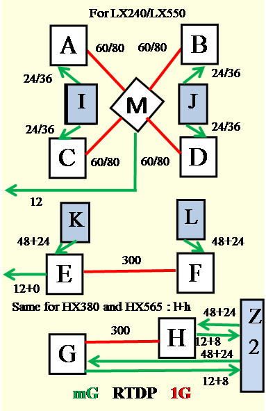
Figure 1 : real-time data path. Green: MGT, red: GPIO
differential
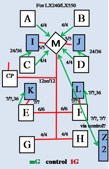
Figure 2 : control and debug path. Green: MGT, red: GPIO
differential
|
MGT1 |
MGT2 |
MGT3 |
GCK1 |
GCK2 |
|
|
|
All LXT |
merger |
All HXT |
All |
All |
|
|
|
|
|
|
|
|
|
|
|
|
|
|
|
|
|
|
|
|
|
|
|
|
|
|
|
|
|
|
|
|
|
|
Table 1 : use of clock connectivity
|
signal |
#pins |
voltage |
|
|
|
|
|
merger |
12 |
2.5 |
|
|
|
|
|
config |
9*7 |
2.5 |
|
|
|
|
|
|
|
|
|
|
|
|
|
|
|
|
|
|
|
|
|
|
|
|
|
|
|
|
Table 2 : use of CPLD connectivity
adapted from JEM requirements…
1.1
Clock
distribution
The clock distribution scheme needs to handle a large variety of signals, both in terms of frequency, signal quality, and signal levels. The application clocks are differential signals. For single-ended FPGA service clocks see section 1.2. Application clocks are generally routed via the clock daughter module. On the main board clock fan-out trees replicate the signals and route them to their final destination. For differential clock lines the general rules on differential controlled impedance lines apply. Clocks are particularly sensitive to impedance mismatches and discontinuities, and in-pair skew.
GCK clocks are LVDS signals. They are fed to their destination FPGAs in a single copy each. MGT clocks are CML signals (???). They need to be AC-coupled upon crossing signal voltage domains and on FPGA inputs. Input biasing schemes are in operation (???). On the FPGAs no more than 3 specified, adjacent MGT quads can be supplied via the clock pad pair of the central quad (???). Therefore multiple MGT clock connections must be made to a single FPGA. The HXT devices must be supplied by separate clock trees for the GTH and the GTX MGT circuits.
The requirements with respect to clock distribution are:
· Receive the following clocks from the clock daughter
o GCK1, GCK2 : LVDS signalling
o MGT1, MGT2, MGT3 : CML 2,5V ?? signalling
· Replicate the GCK clocks and feed them to the following devices in a single copy per FPGA
o GCK1 :
o GCK2 :
· Replicate the MGT clocks and feed them to the FPGAs
o MGT1 :
o MGT2 :
o MGT3 :
· Replicate the MGT clocks such that for the LXT processors the central quad of 3 quads is supplied. This rule must be followed such that the requirements are met, whether the smaller or the larger device is mounted.
· Replicate the MGT clocks such that for the HXT processors the central quad of 3 quads is supplied
· For the Merger FPGA separate rules apply: (check that thoroughly, what do we want?).
o Supply the MTP related quads with MGT1 and … clock
o Supply the SFP related quads with local crystal clocks that allow SFP1 to run at typically 1Gb/s Ethernet rate
o Supply the SFP related quads with local crystal clocks that allow SFP2 and SFP3 to run at 960 Gb/s ROI/DAQ rate
o Supply the SFP related quads with a clock rate suitable for input clock reception at LHC bunch rate multiple for use as TTCRx replacement
· Please note that at current we do not yet know whether the MGTs are suitable for ROI/DAQ and clock handling. We might eventually have to use GPIO lines instead. The data re-routing would have to take place on the clock daughter. However, the necessary clocks should be available at both MGT and GCK pins !
1.2
Configuration and JTAG
On current FPGA families configuration and JTAG interfaces are implemented in in single-ended high-speed low voltage CMOS circuitry.
The requirements with respect to clock distribution are:
·
Route
o Hav
1.3
Board
level issues
:
Power supplies and line impedances
The GOLD is a large, high-density module, carrying large numbers of high-speed signal lines of various signal levels. The module relies on single ended CMOS (2.5 and 3.3V), and differential (LVDS, PECL3.3, PECL2.5, CML3.3, CML2.5) signalling. System noise and signal integrity are crucial factors for successful operation of the module. Noise on operating voltages has to be tightly controlled. To that end, large numbers of decoupling capacitors are required near all active components. FPGAs are particularly prone to generating noise on the supply lines. Their internal SERDES circuitry is highly susceptible to noisy operating voltages, which tend to corrupt their high-speed input signals and compromise the operation of the on-chip PLL, resulting in increased bit error rates. To suppress all spectral components of the supply noise, a combination of distributed capacitance (power planes) and discrete capacitors in the range of nF to hundreds of mF are required.
The GOLD base frequency is 40.00 / 40.08 MHz. Parallel differential I/O operates at multiples up to 1Gb/s. Multi-Gigabit (MGT) links operate at 6.5 or 10Gb/s Those signals are routed over long tracks on-board and across the backplane. This is only possible on matched-impedance lines. Differential sink termination is used throughout. All FPGA inputs are internally terminated to 100Ω or to 50Ω||50Ω, according to the manufacturers guidelines. All lines carrying clock signals must be treated with particular care.
The requirements with respect to signal integrity are:
·
Use low-noise local step-down regulators on the module,
placed far from susceptible components.
·
Observe power ramp and sequence requirements for
FPGAs
·
Run all supply voltages on power planes, facing
a ground plane where possible, to provide sufficient distributed capacitance
·
Provide at least one local decoupling capacitor
for each active component
·
For FPGAs, follow the manufacturer’s guidelines
on staged decoupling capacitors (low ESR) in a range of nF
to mF
·
Observe the capacitance limitations imposed by
the voltage convertors
·
Minimise the number of different VCCO
voltages per FPGA to avoid fragmentation of power planes
·
avoid large numbers of vias
perforating power and ground planes near critical components
·
route single-ended signals on high impedance
lines
·
source-terminate single ended clocks with approximate
impedance
·
Route all differential signals on properly
terminated, controlled-impedance lines:
o Have all micro strip lines face a ground plane
o Have all strip lines face two ground planes or one ground plane and one non-segmented power plane
o
avoid sharply bending signal tracks
o minimise cross talk by running buses as widely spread as possible
o Avoid in-pair skew, in particular for MGT links and clocks
o Avoid impedance discontinuities and stubs, in particular on MGT links and clocks
o
Use LVDS on all general-purpose FPGA-FPGA links
o
Use LVDS on all GCK clock lines
o
Use PECL or CML on all MGT clock lines
o
Use CML on all MGT data lines
o
Use AC coupling on all MGT clock inputs
o
Use AC coupling on all MGT data inputs
o
For all off-board links assume capacitors off-board
o
For on-board links place capacitors close to
source
o
Use AC coupling when crossing PECL/CML domains
o
Use AC coupling when crossing 2.5V/3.3V domains,
except on LVDS
o
Use bias networks on AC coupled inputs where
required
o
Run FPGA configuration and FPGA JTAG clock lines
on 50 W point-to-point source
terminated lines any
better idea? Go differential?
From JEM implementation
details…
1.4
Signal
levels and supply voltages
The GOLD is a mixed signal level environment. Particular
consideration of signal level compatibility and system noise issues is required
so as to make the system work reliably. Differential signalling is employed
throughout the module. Since LVDS, CML and PECL at various signalling voltages
are used, appropriate level translation schemes are used where domains are
crossed. MGT signals and clocks are DC balanced. Therefore capacitive coupling
along with proper biasing networks on the inputs are generally used.
Differential or split / centre tap terminators are employed where input termination
is not provided by the active components.
A very small number of single ended signals is used on the GOLD. Configuration and JTAG lines are high-speed lines and require impedance control and termination. They are all running at the FPGA AUX voltage of 2.5V only. ????
Some amount of slow control lines is run as a mixed 2.5V/3.3V domain. Active level translation is required. As far as possible split supply CPLDs are used to that end.
Module control lines are available in Zone 1 of the ATCA connector. They are routed as high impedance single ended lines to the clock/control module. Some module control functionality as well as DAQ/ROI output was defined by the L1Calo community on a few signal pairs at the bottom of Zone 2. These signals are routed to the clock/control module on differential pairs. Maximum data rate is ~ 1Gb/s.
Power consumption is dominated by the FPGAs. A power budget of ~400W is assumed. The primary supply consists of two -48V/12V bricks.