ATLAS Level-1 Calorimeter Trigger
GOLD Module
-
V1.0-
Project Specification
Version 0.1
Date: 18
November 2010
Uli , Bruno, Eduard
Universität Mainz
1.2.2 Level-2
interface, monitoring, diagnostics, and control
2 Functional
requirements and design issues
2.3 Jet
input data conditioning and energy pre-summation
2.7.1 Playback
and spy functionality
2.8 Board
level issues : Power supplies and line impedances
3.2 Jet
input data conditioning
3.5 FCAL
and endcap calorimeter treatment
3.8 Signal
levels and supply voltages
3.10 Daughter
module iterations
3.11 Summary
of post-FDR design changes
4 Interfaces
: connectors, pinouts, data formats
4.2 backplane
connector layout
1
Introduction
This document describes the specification for the initial version 1.0 of the Generic Opto Link Demonstrator (GOLD). The specifications cover the processor board as well as daughter modules carrying clock circuitry and opto-electrical receivers. Section 1 of this document gives an overview of the module. Section 2 describes the functional requirements. Section 3 details the implementation.
1.1 Related projects
The GOLD is a demonstrator for the Topological Processor module and is therefore a major processor module within the Cluster and Jet processor scheme of the ATLAS level-1 calorimeter trigger. The Topological Processor will be located between the CMM++ and the CTP in the L1Calo architecture. A demonstrator for the CMM++ is the BLT. The future CTP is assumed to be electrically identical to its current incarnation, the firmware, and the data formats on the interfaces might be different.
TTC http://www.cern.ch/TTC/intro.html
Current L1Calo modules http://hepwww.rl.ac.uk/Atlas-L1/Modules/Modules.html
TTCDec http://hepwww.rl.ac.uk/Atlas-L1/Modules/Components.html
CTP
1.2
Overview
The Topological Processor within the L1Calo architecture is a single processor crate equipped with one or more processor modules. The processor modules will either be identical copies with firmware adapted to the specific topologies to operate on. Alternatively it could be modules tailored to a specific topology in hardware. The GOLD is a first technology demonstrator for the topological processor and other future L1Calo modules. These specifications describe its use as a Topological Processor demonstrator only. It is meant to be operated on output signals of a first prototype of the CMM++, or initially on the BLT.
The GOLD will receive the topological output data of the sliding windows processors. The details of the data formats are not currently known. However, the information transmitted into the GOLD will be basically comprised of the ROI data that are currently transmitted to the 2nd level trigger. The data will consist of a description of the position of an object (jet, e/m cluster, and tau) along with some qualifying information, basically the energy sum within the object. Preliminary data formats have been devised. Data are going to be transmitted on optical fibres. After conversion to electrical representation, data are received and processed in FPGAs. Results are sent to the Central Trigger processor.
1.2.1
Real-time
data path
The GOLD is a module in ATCA form factor. Backplane zones 2 and 3 are used for real-time data transmission. The module incorporates two distinct processing schemes. One is based on currently available FPGAs (XC6VLXT series), the other one tries to make use of FPGAs (XC6VHXT) meant to be available very soon. The baseline operation of the GOLD relies on the LXT scheme. The HXT FPGAs will not be mounted initially.
The CMM++ data enter the GOLD optically through the backplane. The fibres are fed via five blind-mate backplane connectors that can carry up to 72 fibres each. That limits the maximum aggregate bandwidth to 3.6Tb line rate, if 10 Gb/s transmission is used throughout. Initially, however, the interfaces will be used at lower rates, and with just 12 fibres per connector. The optical signals are converted to electrical signals in 12-fibre receivers. Data reception is handled on a daughter module, stacked on the component side of the GOLD. The GOLD mainboard is fed with electrical signals, which are routed through a total of four industry-standard FMC connectors with differential signal layout. The data are routed to four FPGAs, where they are de-serialised in MGT receivers; the parallel data are presented to the FPGA fabric. In the four input processors part of the algorithms are run, the actual topological algorithms requiring access to data from the full eta/phi space of L1Calo, however, are run on the main processor chip. The final results are transmitted towards the CTP on optical fibres. The signals are converted electrical and de-serialised with low latency receivers on an adapter module located near the CTP crate.
The operation of the real-time data path requires low-jitter clocks throughout the system. For synchronous operation, data transmitters will have to be operated with clean multiples of the LHC bunch clock. Receiver reference clocks may as well be derived from local crystal oscillators, though tight limits on the frequency range will have to be observed. The module will be designed for 40.08 MHz operation only.
1.2.1.1
Input
processing
The optical data arrive on the input daughter module on standard 12-fibre bundles. Since the backplane connectors support multiples of 12 fibres, the signals might in a future version of the board be supplied by “octopus” cable sets, splitting 24, 36, 48, or 72 fibres into groups of 12. It should be noted that un-armed, bare fibre bundles are very flexible and can easily be routed to their destination, even in high-density designs. However, they need to be protected from mechanical stress. The opto-electrical conversion will be performed in AVAGO or compatible 12-channel devices. Industry-standard SNAP12 devices are not considered an option, since so far no high-bandwidth devices are available from any supplier. The opto receivers exhibit programmable pre-emphasis so as to allow for improvement on signal integrity for given track length.
Since the number of input channels will be higher than the number of optical inputs initially, the electrical signals are routed from the o/e converters into CML fan-outs, and then onto the daughter connectors. While the daughter module concept with a rather inexpensive and almost passive (except the fan-outs) carrier for the opto receivers is particularly useful in the demonstrator and prototyping phase, it is envisaged for the production modules as well. Such a concept allows for several instances of a topological processor to be run with different signal routing, optimised for the respective algorithms. The CML circuits do not allow for neither pre-emphasis nor signal equalisation. Therefore signal conditioning on the data sources and sinks are required, if longer tracks are to be used.
On the main board the multi-gigabit links are de-serialised on the input processors. They allow for programmable signal equalization on their inputs. The exact data formats are as yet unknown, though standard 8b/10b encoding is envisaged for purpose of run length limitation and DC balance. The processors are supplied with required bias and termination voltages, as well as a suitable reference clock.
The input processors are assumed to do some local pre-processing on the incoming data. The extent of local processing is determined by the respective algorithms.
1.2.1.2
Main
processor
The main processor has accesses to data from the full solid angle in eta and phi. Data volumes are limited by the general purpose I/O bandwidth of the FPGA. In the first iteration of the module a XC6VXLX240 is used. With a line rate of 1Gb/s and a total of 240 differential lanes into the main processor the aggregate bandwidth is limited to 240 Gb/s. This theoretical limit cannot probably be reached, since a fraction of lanes might be required for control purposes, as the main processor dubs as a module controller. Bandwidth can be increased when larger, foot print compatible FPGAs are mounted on the PCB. The use of multi-Gigabit links on this path is not effective due to their higher latencies. 600-lane FPGAs of the XC6V series have been announced, but are not yet available. Due to the currently limited aggregate bandwidth of parallel I/O the results of the topological algorithms are sent on to the Central Trigger Processor on multi-gigabit links. A single fibre-optical ribbon connection through the front panel of the module is provided for this purpose. An adapter board will be required to interface the GOLD to the LVDS inputs of the current CTP. This module will be equipped with CML-to-LVDS de-serialisers DS32EL0124 or similar.
1.2.1
Clock
distribution
Both the FPGA fabric and the multi-Gigabit transceivers (MGT) need to be supplied with low latency clock signals of appropriate signal levels and signal quality. The fabric clocks are multiples of the LHC bunch clock at LVDS levels. The MGT clocks are CML level signals, AC-coupled into the MGT clock pads of the FPGAs. The jitter of the MGT clocks has to be tightly controlled. Clock generation and jitter clean-up are performed on a clock and control daughter module, located towards the bottom of the GOLD. The clock distribution trees are located on the GOLD main board. The clock fan-out chips chosen are devices with multiple signal level input compatibility, and output levels suitable for their respective use, either LVDS or CML. The devices are manufactured by Micrel.
There are two independent clock trees for the fabric clocks into all FPGAs. There is one common MGT clock tree into all FPGAs. Another MGT clock tree supplies all XC6VLXT devices. There is yet another clock tree available to supply the XC6VHXT devices (see below).
he data rates envisaged are up to 6.5Gb/s, or about 10Gb/s. These bit rate domains are dictated by the FPGAs to be used. The data rates are currently assumed to be multiples of the LHC bunch clock rate. This would allow for synchronous operation of the module.
ta from the Pre-processor are received on serial links at a rate[1] of 400Mb/s (Figure 1). On the JEM the data are deserialised to 10-bit words (9-bit energies with odd parity bit) at the LHC bunch clock rate of 40.08 MHz[2]. These data are presented to a first processor stage consisting of a bank of input processor FPGAs, located on daughter modules R, S, T, U. The data are first phase corrected and checked for errors (Figure 2). The electromagnetic (em) and hadronic (had) values for each trigger tower are then summed into 10-bit jet elements. The jet element values are multiplexed to twice the bunch clock rate and sent to the jet processor FPGAs. Because the jet algorithm uses data from a 4´4-bin neighbourhood around each processed jet element (see sect.2), neighbouring JEMs share data via fan in/out (FIO) links on the backplane. To accomplish this, the input processors send copies of shared jet elements to the neighbouring modules. Three out of four jet elements are duplicated in this manner.
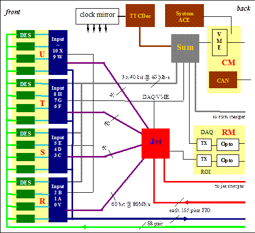
Figure 1: Block diagram of JEM, including daughter modules R,S,T,U, RM, CM, TTCDec
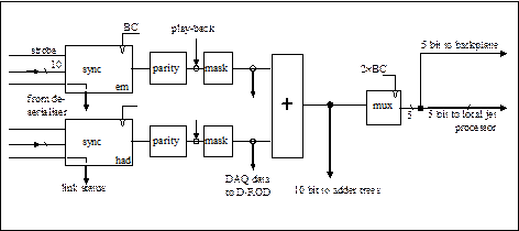
Figure 2 : JEM input processor : jet element formation, one out of 44 jet elements shown
The jet algorithm uses jet elements received from the local input processors as well as overlap data from neighbouring JEMs. To process a core of 8´4 potential jet positions, an environment of 11´7 jet elements is required. Within this environment the jet processor FPGA identifies and counts clusters of 2´2, 3´3, and/or 4´4 jet elements around a 2´2 local maximum that exceeds one of 8 programmable thresholds, and reports the to the jet CMM in the form of eight 3-bit multiplicities[3], plus 1 bit of odd parity.
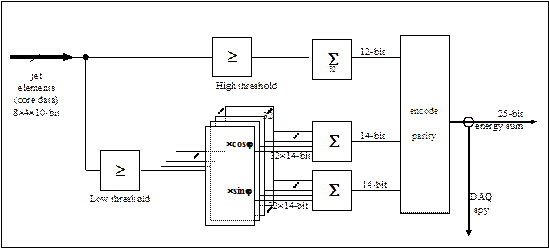
Figure 3 : JEM energy processing
The energy algorithm operates on the 32 core jet elements. The sum trees span input processors and sum processor (Figure 3). Total transverse energy is determined from a scalar sum over all core jet elements, while missing transverse energy is determined from a vector sum. A low threshold is applied to the jet elements on the missing energy data path. A separate threshold is applied to data entering the transverse energy adder tree. The jet elements are converted to x and y projections by multiplication with cosine and sine of j, respectively. The vectors results are summed and transmitted along with the scalar transverse energy to the energy summation CMM as a 25-bit (odd) parity-protected data word.
Energy summation is performed with a precision of 1 GeV for the transverse energy and 0.25 GeV for the projections. The energy range is 4095GeV. Signals exceeding full scale are saturated to 4095GeV. Due to limitations on backplane bandwidth only 8 bits of data are available for each of the energy data words. Therefore a compression scheme is employed that ensures 1 GeV resolution for small signals while accommodating the full 4095GeV range.
1.2.2
Level-2
interface, monitoring, diagnostics, and control
To help the Level-2 trigger efficiently evaluate events accepted by Level-1, the Level-1 trigger provides information on regions of interest (RoI) identified by the real-time data path. In the JEM, the RoI information comprises the coordinates and types of jets identified in the processor FPGA. The readout of ROI information is initiated by a Level-1 accept signal, which is asserted by the CTP several bunch crossings after the event has been processed in the real-time data path of the JEM. This latency is compensated by a shift register (latency buffer) that delays the RoI data and brings them in phase with the Level-1 accept signal. The latency-corrected RoI data is written to a FIFO (derandomiser buffer) upon receipt of a Level-1Accept signal. The RoI data is then serialised to a 40Mb/s bit stream and sent via a read-out controller (ROC, implemented on the jet processor), 800 Mb/s serial links[4] and optical transmitters (located on the read-out daughter module RM, Figure 1) to R-RODS which forward the data to the level-2 trigger (see Figure 4, readout related paths shown in black).
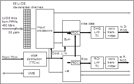
Figure 4: RoI and DAQ slice data path
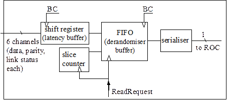
Figure 5 : Input processor : readout sequencer
Provision is made for extensive monitoring via the ATLAS data acquisition system. All real-time data entering or leaving the processor modules via cables or long backplane links are stored in latency buffers (Figure 7) for eventual readout to the DAQ for all LVL-1 accepted events. The derandomiser buffer captures data from 1 to 5 bunch crossings for each accepted event, and serialises the data to a 40Mb/s bit stream.
On each JEM there are 16 sources of bit-serial DAQ data. The input processors contribute a total of 15 bit streams containing the data received from the de-serialiser chips (for the data format see Figure 10). The jet and sum processors contribute one bit stream of data, describing the jet and energy sum signals sent to the merger modules. The bunch count information is included in the bit stream as well. The 16-bit data words are forwarded to D-RODs via a 800Mb/s link chip and an opto transmitter.
For diagnostic purposes, additional playback and spy memories are provided. The playback memories can be filled with test patterns under VME control. VME controls the insertion of the playback data into the processing chain (Figure 2). Data downstream of the playback memories are captured into spy memories (Figure 3) that can be read out via VME for analysis. The pointers to all playback and spy memories are aligned upon receipt of a synchronous command, broadcast by the TTC system.
The main control path for the JEM is via a bus that carries a reduced set of VME commands. The physical interface is an A24D16 bus with a very small number of control lines. Signal levels are 3.3V CMOS. Programmable logic is used to interface the reduced VME bus to the JEM processor chips.
Environmental data are monitored by the DCS (detector control system). The JEM communicates with DCS using a local microcontroller-based CAN node (Figure 1, control daughter module CM). The controller collects temperature and supply voltage data, and forwards them to a crate-level master device via a 2-pin CAN link on the processor backplane.
The JEM processor chips are programmable devices with volatile firmware storage. Therefore, hardware is required to download configuration code to the devices upon power-up. Configuration data is supplied by a compact-flash card (Xilinx System ACE ) allowing for the storage of multiple configurations for each device.
System timing is derived from a TTC signal distributed to every module in the system. A single TTCrx chip on each JEM provides bunch clock signals, trigger information and synchronous and asynchronous control commands.
2
Functional
requirements and design issues
The role of the JEP is to derive total transverse energy, missing transverse energy, and jet multiplicities from data provided by the PPr. The JEM covers the first stages of the jet and energy algorithms within a trigger space of 8 bins in j ´ 4 bins in h. The full real-time jet and energy processing chain includes the JEM and two stages of CMMs. All data processing functions are implemented in FPGAs, using a fully synchronous design, with I/O flip-flops used throughout. The JEM is linked to DAQ and LVL-2 via front panel optical connectors. All other signals are routed through the backplane on 2mm pitch PCI-type connectors.
This section outlines the requirements for all functions of the JEM. Implementation details are located in Section 2.8 of this document. For information on interfaces with other system components, see section 4.
2.1
Arithmetic
The jet and energy algorithms described below operate on energy data, represented by integer values. Missing energy vectors are real numbers due to the multiplication of transverse energies with real coefficients (sin or cos φ)
The requirements are:
- Calculate all transverse energies at an accuracy of 1GeV per bit
- Approximate real numbers by integers at an accuracy of 0.25GeV per bit
- Detect overflows throughout the algorithm
- When an overflow is detected set the result to the maximum value (saturate)
- Whenever one or more input signals are saturated, propagate the saturation to the output
2.2
Jet
input data reception
The JEM receives energy data from the PPr (see Figure 7) via 88 serial link channels at a data rate of 400 Mb/s. The input signals enter the JEM through the backplane. They are routed to input daughter modules, 24 channels per module, four modules per JEM. The serial data stream is converted to a 10-bit parallel stream by 6-channel LVDS deserialisers ( SCAN921260, compatible to DS92LV1021). The data word is accompanied by a link status bit. For data format details, see section 4.
The requirements on the JEM with respect to jet data reception are:
- Receive differential 400 Mb/s LVDS signals from the backplane on matched-impedance lines[5]
- Feed the serial lines to the deserialisers
- Provide the deserialisers with a reference clock
- Route 10 data bits and link status from each deserialiser channel to an input processor FPGA at the bunch clock rate.
2.3
Jet
input data conditioning and energy pre-summation
Both the jet and the energy algorithms operate on jet elements of 0.2´0.2 (j´h) bin size. They require information on the total energy deposit per bin. Therefore it is convenient to send the raw data words through an initial processing stage that is common to both jet and energy algorithms. This includes data re-timing, bit error handling and an initial summation of the electromagnetic and hadronic data in each jet element. Faulty or unused[6] channels are suppressed, as well as energy sums below a programmable threshold. If at least one of the electromagnetic or hadronic energy values is saturated (at the maximum value), the jet element energy sum is set to its maximum value. The jet element data are multiplexed to 5-bit wide data streams at twice the bunch clock rate, for transmission to the jet processor stage.
Energies are pre-summed on the input processors and sent to the sum processor.
The requirements for jet element formation and energy summation are:
· Receive 10 bits of data (9 bits plus odd parity) and a link status bit from each deserialiser channel
· Latch the data and status into input flip-flops, two samples per bunch tick.
· Select the stable one of the two samples under software control (phase select).
· Mask out (zeroing data and status bits) faulty data channels (LVDS link failures) using a VME-controlled register.
· On a link error, zero the corresponding data word and count the error for monitoring purposes.
· Calculate odd parity of the 9 data bits from each deserialiser channel, and compare it with the parity bit.
· On a parity error, zero the corresponding data word and record the error for monitoring purposes
· Add electromagnetic and corresponding hadronic energy into a 10-bit wide jet element.
· Set the jet element to maximum value if at least one of the deserialiser data values is at maximum.
· Multiplex jet elements to 5-bit data at twice the bunch clock rate (least significant bits first)
· Duplicate three out of four jet elements to send copies to neighbouring JEMs
· Subject jet elements to a VME-programmable low threshold. Jet elements below this threshold are zeroed.
· Calculate EX and EY from jet elements at 0.25 GeV accuracy using 12-bit coefficients loaded from the data base[7].
· Sum EX and EY to 14-bit numbers.
· Subject the jet elements to a programmable high threshold
· Sum jet elements to 12-bit transverse energy sum.
· Add pipeline flip-flops in the algorithm at appropriate depths to guarantee reliable operation at the required clock rate
· Latch all output data on output flip-flops
· Transmit four 5-bit streams per φ-bin to the jet processor, two to the left hand neighbour JEM, one to the right hand side.
· Transmit a total of 40 bits (12+14+14) to the sum processor.
2.4 Sum processing
Each JEM processes a core area of 8 j-bins by 4h-bins of the jet/energy trigger space. The energy sum processor performs the final summation of pre-summed energies received from 3 of the 4 input processors, covering the core area. The three resulting energy sums need to be compressed to a 24-bit data word. The baseline algorithm utilises a quad-linear encoding scheme. The energy data words are driven down the JEP backplane, accompanied by one (odd) parity bit.
The requirements for the energy sum processor are:
· Receive 40 bit of energy data (12,14,14 bits of ET,EX,EY) from each of the input processors R,S,T
· Latch data at the bunch clock rate in input flip-flops and route to the adder trees
· add three 12-bit transverse energies (1GeV resolution)
· add three 14-bit missing energy vectors (EX,EY) at a resolution of 0.25GeV
· cut EX and EY to 12 bits each, 1GeV resolution
· Compress the energy sums and encode them to a 25-bit odd parity-protected data word
· Latch all output data on output flip-flops before sending them across the backplane
2.5
Jet
processing
Each JEM processes a core area of 8 j-bins by 4 h-bins of the jet trigger space, within an environment of 11´7 jet elements required by the jet algorithm. Since jet elements are transmitted as 5-bit data at twice the bunch clock rate, the jet processor FPGA requires a total of 385 input data lines. The jet processor produces 24 bits of result data, representing 3-bit jet multiplicities for 8 thresholds, along with one (odd) parity bit. The result data words from all JEMs are transmitted via point-to-point backplane links to the Jet CMM.
The requirements for jet element and results handling are:
· Provide a synchronous local clock at twice the bunch clock rate
· Receive 44 5-bit jet elements from local input processors at twice the bunch clock rate, with the 5 least significant bits arriving first
· Receive 22 jet elements from the neighbouring JEM on the right, and 11 jet elements from the left
· Latch the jet elements in input flip-flops at twice the bunch clock rate with a programmable phase (Clock40Des2)
· Demultiplex jet elements and retime at the bunch clock rate
· Subject the jet elements to a programmable threshold
· Identify FCAL elements by the module geographic address and channel number, and map them to the central jet element granularity by dividing the energies by 2, and populating two adjacent cells with 0.1´0.1 granularity (see sect. 3.5)
· Supply the jet algorithm with 77 10-bit wide jet elements.
· Receive 24 bits of jet count data at the bunch clock rate from the jet algorithm
· Encode them to a 25-bit odd parity protected data word
· Latch all output data on output flip-flops before sending them across the backplane to the jet CMM.
The Jet algorithm identifies and counts clusters of jet elements centred around a local maximum that exceed one or more programmable thresholds. The jet algorithm supports eight independent jet definitions, each consisting of a programmable threshold associated with a selectable cluster size. Jet elements are first passed through a summation algorithm, which produces energy sums for 60 (6x10) 2x2 clusters, 45 (5x9) 3x3 clusters, and 32 (4x8) 4x4 clusters. Cluster sums containing saturated jet elements are flagged. The central 32 (4x8) 2x2 clusters are compared with their nearest neighbours to determine whether they are local maxima, and therefore possible jet candidates.
The central 4x8 region processed by each Jet FPGA is divided into eight 2x2 subregions, each of which can contain no more than one local maximum. When a local maximum is identified in a subregion, the 2x2, 3x3, and 4x4 clusters associated with it are selected and compared with appropriate thresholds. If no local maximum is found, the output of the subregion is zeroed. Clusters, associated with local maximum, which contain saturated elements automatically pass all enabled thresholds. For JEMs covering only the central calorimeter, three-bit multiplicities of jet clusters satisfying each of the eight jet definitions are produced. JEMs servicing both the FCAL and central calorimeter produce eight 2-bit central jet multiplicities, and four 2-bit FCAL jet multiplicities.
The location of the jet cluster within each 2x2 subregion, its associated threshold bits and a saturation-flag are stored in a variable-length pipeline for readout to the ROI builder upon a Level-1 accept.
The requirements for the jet algorithm are:
· Receive 77 jet elements 10-bit, FCAL energies divided evenly between two neighbouring jet elements in j
· Produce sums of 2x2, 3x3, and 4x4 jet elements.
· Identify 2x2 ROI candidates that are a local maximum
· Select ROI candidate coordinates within each 2x2 subregion
· Compare 2x2, 3x3, and 4x4 candidates against 8 programmable size/energy thresholds
· Produce 8 3-bit jet multiplicities corresponding to ROI candidates satisfying each of the 8 programmable thresholds for JEMs covering the central calorimeters
· Produce 8 2-bit central jet multiplicities and 4 2-bit FCAL jet multiplicities for JEMs covering both the central calorimeters and FCAL.
· Output these multiplicities at the bunch clock rate
· Output ROI coordinate and threshold bits (plus saturation bit) at the bunch clock rate to be entered in the ROI readout pipeline.
2.6
DAQ
and RoI
All real-time data (slice data) crossing board boundaries on long backplane links or cables are captured on the inputs or outputs of the processor chips and stored there in latency buffers to await a Level-1 accept decision. Duplicated data shared between neighbouring JEMs is not recorded in this way, due to the large number of bits involved. Bunch crossing identifiers are recorded along with the slice data. Upon a positive L1A decision, up to 5 consecutive bunch clock ticks worth of data are transferred to a derandomising FIFO buffer, from which they are serialised to one-bit wide data streams at the bunch clock rate. Data from accepted events are sent to the DAQ for subsequent data analysis and validation.
Jet coordinates indicating regions of interest (RoI) are captured and read out by the jet processor FPGA by a readout structure similar to the one above. Upon a L1A, a single time slice of data is derandomised, serialised, and forwarded to the Level-2 trigger.
The readout pipelines and derandomisers are implemented locally on the processor chips. The buffers are controlled and read out by local readout sequencers (R/S), that communicate with a readout controller (ROC) that collects the single-bit data streams. The ROC formats the data and sends it off-board to readout drivers (D-RODs, R-RODs) over 800 Mb/s serial links and electro/optical converters, located on a readout daughter module(RM).
The requirements with respect to DAQ and RoI data processing are:
· Sample all critical real-time JEM input and output slice data, including:
o incoming LVDS-link data including link status bit (24´11-bit per input processor FPGA)
o a 12 bit bunch count identifier
o outgoing trigger data
- 24 bits of jet count information plus 1 (odd) parity bit
- 24 bits of energy sum information plus 1 parity bit
· record the jet coordinates found by the jet processor (8 jets, each with 2 position bits, 1 saturation bit and 8 threshold bits)
· pipeline the slice and RoI data for a fixed number (approximately 48)[8] of bunch clock ticks corresponding to the maximum possible downstream latency before L1A reception
· derive a ReadRequest signal from the LVL-1 accept signal with a programmable offset of up to 63 bunch clock ticks to compensate for possible varying downstream latencies
· assert the ReadRequest signal for 1 to 5 bunch clock ticks
· read out the pipeline data to 256-deep FIFOs on ReadRequest:
o 1 to 5 consecutive data words for slice data
o 1 data word for RoI data
· serialise the DAQ data to 16 single-bit data streams:
o four data streams per input processor R,S,T
o three data streams per input processor U
o one data stream for jet count, energy sum data and for the bunch count identifier data
· serialise the RoI data to a two-bit data stream (4 bit wide for FCAL JEMs)
· Begin transmission of data streams immediately on ReadRequest if the FIFOs are empty
· continue data transmission until FIFOs are empty
· separate data from consecutive events by at least one empty separator bit[9]
o slice data packets are 1-5 ´ 67 bits long (including parity)
o ROI data packets are 45 bits long (including parity)
· collect the data streams in the ROCs
· ( re- ) synchronise the readout data to a local 40 MHz crystal clock
· Provide link chips with a clean crystal clock
· present slice data and bunch count identifier to the DAQ link chip (16-bit wide)
· present RoI data and bunch count identifier to the RoI link chip (3/5-bit wide)
· use a link chip compatible to HDMP1022 16-bit mode, FF1, alternating flag as specified in http://cp.literature.agilent.com/litweb/pdf/5989-0352EN.pdf
· send fill-frames (FF1) rather than data when no data are available or when a link separator bit is received[10].
2.7
Diagnostics
and control
2.7.1
Playback
and spy functionality
The JEM allows stand-alone diagnostics of the data path using dual-ported play-back memories to feed test patterns into the input processors. The patterns are processed in the data path, and the results are captured by spy memories further down the chain. Both types of diagnostic memories are accessible via VME. Playback and spy mode are enabled via VME. The pointers are aligned by a TTC short broadcast command.
The requirements with respect to diagnostics are:
· provide 256-deep playback buffer memories in the input processors, 9-bits wide for each input channel
· Load test patterns into the VME port of the play-back memory. Memory write addresses are incremented on each VME write operation
· Under VME control start or stop capturing data in the spy memories
· Under VME control start or stop injecting playback data into the real-time data path
· provide 256-deep 24´10-bit wide spy buffer memories in the input processors
· provide 256-deep 25-bit wide spy buffer memories in the sum processor
· provide 256-deep 25-bit wide spy buffer memories in the jet processor
· read out spy memories through the VME port. Memory read addresses are incremented on each VME read operation
· Upon receipt of a short broadcast command from the TTC system, reset the pointer to the real-time port of the memories
2.7.2
VME
interface
Main board control is performed through a reduced width, reduced functionality VME-- bus running on the JEP backplane (Table 4, for pin-out see sect. 4.2). The 3.3V CMOS backplane signals are interfaced to the processors via buffers and a VME controller located on the sum FPGA (for details see sect.2.8). An additional non-volatile CPLD allows restricted VME access to the module when the FPGAs are unconfigured. The sole purpose of this CPLD is to allow for VME-controlled reconfiguration, should there be problems with automatic FPGA configuration after power-up. Module addresses are read from geographic addresses encoded on backplane pins GEOADD0 ... GEOADD5.
The requirements with respect to VME control are:
· provide the module with limited D16/A24 VME access
· buffer all bus signals in compliant transceivers (3.3V CMOS), keep stubs short
· implement a set of basic functions in a non-volatile control CPLD:
o derive the module base address from geographic addressing
o decode the module sub-address range
o respond with DTACK to all D16/A24 commands referring to the module sub-address
o allow for control of the SystemACE chip so as to force FPGA reconfiguration
o provide registers for sum FPGA configuration download via VME (debug feature only)
· connect the VME bus to the VME controller on the sum FPGA
· control the processor FPGAs through the VME controller, mapping the processor control and status registers to the module VME sub-address space
2.7.3
DCS
interface
Environmental variables are monitored through the DCS system. The JEM is linked to DCS through a single CAN signal pair serving all modules on the processor backplane.
The requirements with respect to DCS control are:
· provide CAN access via the backplane
· run the CAN signal pair through a CAN PHY (physical layer interface) to a local CAN controller.
· supply the CAN controller with a node address derived from the geographic addresses in the control CPLD
· use a CAN controller compliant with L1Calo CAN specifications
· have the CAN controller monitor all module supply voltages and temperatures on selected FPGAs.
2.7.4
JTAG
port
JTAG access is required for board and chip test and for downloading CPLD and FPGA configurations. The JEM provides separate JTAG chains for CPLDs, FPGAs and non-programmable logic. The chains are routed to a common multi-pin connector where they can be joined, if required. All scanable devices are connected to one of the chains.
The requirements with respect to JTAG are:
· link all CPLDs to a single JTAG chain and route to the JTAG connector
· link all FPGAs to a single JTAG chain and route to the secondary port of the system ACE chip. Route TCLK of this chain such that ringing is minimised.
· route the system ACE primary JTAG port to the JTAG connector
· link all buffers to a single JTAG chain and route to the JTAG connector
· link all LVDS deserialisers to a single JTAG chain and route to the JTAG connector
· link TTCDec and G-link module to a single JTAG chain and route to the JTAG connector
· provide access to the chain with a JTAG header via buffers
2.7.5
Configuration
All FPGAs must be supplied with a configuration data stream upon power-up of the JEM. CPLDs are configured by non-volatile on-chip memories, and require a configuration data stream only for initial setup and later firmware updates. Non-volatile memories on the JEM store FPGA configurations for automatic configuration during power-up. Xilinx System ACE is used for this purpose. It consists of an ASIC and a standard compact-flash card socket. It interfaces to the processors via JTAG.
For debug purposes configurations can be loaded via VME. The VME controller connects to the slave-mode configuration ports of all FPGAs. All input processor FPGAs on a JEM share the same configuration, and are therefore loaded in parallel from a single data stream. Sum and jet processor FPGAs receive separate streams. Configuration data streams are typically of the order of one or more MBytes each.
The requirements with respect to configuration are:
· provide on-board Xilinx System ACE (chip and card socket) for flash-configuration
· provide the SystemACE chip with a clean local crystal clock
· link ACE to external JTAG port and to the processor chain
· link ACE to the local VME subsystem
· allow for automatic configuration via SystemACE upon power-up
· allow for reconfiguration under VME control
· allow for automatic slot dependent selection of a set of firmware
· provide a CPLD based sequencer to generate data streams and accompanying clocks
· control FPGA mode pins to enable slave parallel or serial configuration
· feed FPGA CCLK and DIN pins with configuration clocks and data
· feed identical copies of configuration stream to the 4 input processors
· feed individual data streams to sum and jet processor
· monitor successful configuration and report status to VME
2.7.6
TTC
interface
Timing and control information is received through the TTC system. A 160 Mbit/s TTC data stream is received on a single signal pair from the processor backplane. Bunch clock, bunch crossing and event number as well as Level-1 Accept and other broadcast signals are decoded by a TTCrx (TTCDec) module and are supplied to the processor chips through the sum FPGA.
The requirements with respect to TTC signal processing are:
· receive TTC signals from the backplane on a differential pair
· terminate (100R) and refresh them in a line receiver (LVPECL) close to the backplane
· route them to a TTCDec module on a 100R differential line
· supply the TTCDec with a reset signal from the sum FPGA
· supply the TTCDec with parallel configuration data upon reset
· supply the TTCDec with a configuration data stream (I2C) from the sum FPGA
· decode the TTC signals in the TTCDec
· supply all processor FPGAs with the buffered, source terminated Clock40Des1 bunch clock signal
· supply the jet processor with the Clock40Des2 bunch clock signal
· allow for supply of the sum FPGA with all parallel TTCrx signals (optional[11])
2.8 Board level issues :
Power supplies and line impedances
The JEM is a large, high-density module, carrying large numbers of high-speed signal lines of various signal levels. The module relies on TTL, PECL, current mode (LVDS) and CMOS high- and low swing signalling. System noise and signal integrity are crucial factors for successful operation of the module. Noise on operating voltages has to be tightly controlled. To that end, large numbers of decoupling capacitors are required near all active components. Virtex FPGAs are particularly prone to generating noise on the supply lines. The LVDS deserialiser chips are highly susceptible to noisy operating voltages, which tend to corrupt their high-speed input signals and compromise the operation of the on-chip PLL, resulting in increased bit error rates. To suppress all spectral components of the supply noise, a combination of distributed capacitance (power planes) and discrete capacitors in the range of nF to hundreds of mF are required.
The JEM operates mainly at data rates of 40 and 80 Mb/s. Serial links of 400 and 640 Mb/s data rate are used on the real-time data path and DAQ/LVL2 interfaces. Those signals are routed over long tracks on-board, across the backplane, or over cables. This is only possible on matched-impedance lines. Depending on the signal type, differential sink-terminated and single-ended source-terminated signal lines are used. Micro strip and strip line technologies are used for signal tracks. All lines carrying clock signals must be treated with particular care.
The requirements with respect to signal integrity are:
·
use low-noise local
step-down regulators on the module, placed far from susceptible components.
Observe ramp-up requirements for Virtex-II
·
use external 3.3V
supply for the LVDS links.
·
run all supply voltages on power planes, facing
a ground plane where possible, to provide sufficient distributed capacitance
·
Provide at least one local decoupling capacitor
for each active component
·
For de-serialiser
chips and for Virtex-2, follow the manufacturer’s guidelines on staged
decoupling capacitors (low ESR) in a range of nF to
mF
·
Observe the capacitance limitations imposed by
the voltage convertors (10mF)
·
Minimise the number of different VCCO
voltages per FPGA to avoid fragmentation of power planes
·
avoid large numbers of vias
perforating power and ground planes near critical components
·
Route all long-distance high-speed signals on
properly terminated, controlled-impedance lines:
o
Use DCI source termination on all single-ended
FPGA outputs
o
Route 400Mb/s input signals to de-serialiser chips on short micro-strip lines of 100 W differential mode impedance with 100 W sink termination
o
Route TTC input signal pairs on 100 W micro-strip lines
with 100 W
sink termination
o
Route DAQ and RoI
serialised signals on short 100 W differential micro-strip lines.
o
Route 80 Mb/s JEM-JEM FIO lines on
source-terminated 60 W
strip lines or micro-strip lines
o
Route 40 Mb/s merger lines on source-terminated
60 W
strip lines or micro-strip lines
o
Route long-distance bunch clock signals on
source terminated single ended 60 W lines
o
Run FPGA configuration and FPGA JTAG clock lines
on 60 W
point-to-point source terminated lines
·
have all micro strip lines facing one ground
plane
·
have all strip lines facing two ground planes or
one ground plane and one continuous power plane
·
avoid sharply bending signal tracks
·
minimise cross talk by running buses as widely
spread as possible
·
minimise the lengths of all non-terminated
high-speed signal lines
·
use the TTCdec PLLs in
conjunction with low-skew clock drivers to generate symmetric, low-noise,
low-skew bunch clock signals
·
route all clocks into global clock pads
(FPGA,CPLD)
· route CAN signals on short, unterminated stubs.
3
Implementation
The JEM is a largely FPGA-based processor module designed to minimise latency of the real-time path of data flowing from the pre-processor to the central trigger processor. Data processing is performed at a data rate of 40 Mb/s in a pipelined processor. Input data are de-serialised from 400 Mb/s streams to 10-bit parallel words upon entrance into the module. Output to the CTP is sent via merger modules at the bunch clock rate. Jet element data are shared with neighbouring modules at twice the bunch clock rate.
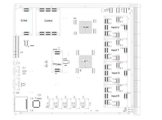
Figure 6 : JEM drawing
Most signals enter and leave the JEM through rear edge connectors via a backplane (common processor backplane, PB). High-speed input data are received on cable links connected to the backplane and brought directly to the module. The JEM is connected to the backplane through 820 signal and ground pins, plus three high-current power pins.
The JEM is a 9U (366mm) high and 40cm deep module that fits a standard 9U 21-slot crate with IEEE 1101.10 mechanics. The module is mechanically strengthened with help of bracing bars along the top, the bottom, and the backplane. ESD strips are provided at top and bottom, connected to signal ground via 1M resistors. The front panel is not electrically connected to the JEM and will be grounded through the crate mechanics only. The module is built on a 14-layer PCB with ground and power planes and impedance-controlled stripline and microstrip layers. While the jet processor and the energy sum processor are mounted on the 9U PCB, the input processors (R,S,T,U), as well as the readout link chips (RM) and control circuits (CM) and the clock circuitry (TTCdec) are located on daughter modules, attached with SAMTEC high-density connectors. Differential LVDS signals are routed on dedicated differential connectors with well-defined differential impedance. The modular design has been chosen so as to limit the number of signal layers required in the highly congested areas around the input processors. Here a large fraction of routing is local connectivity from the deserialisers to the FPGAs. These signals are run locally on the input modules (12 layers). At the time of main board design for the production modules G-link and CAN/control circuitry were not finalised and were therefore implemented on daughter cards as well (RM 4 layers, CM 6 layers). The TTCdec module is a common component and is used on all calorimeter trigger processors.
Table 1 shows processor details, resource use and the timing margins for the current latency. The latency for energy and jet path is measured from the start of an incoming LVDS data word to the start of the corresponding merger output word, as measured on the backplane connector.
|
Processor type |
Processors per JEM |
Device |
slices |
RAMs |
Multi-plier |
Maximum clock |
Latency |
|
Input |
4 |
XC2V1500-4FF896 |
72% |
75% |
50% |
43.1 MHz |
|
|
Sum |
1 |
XC2V2000-4BG957 |
15% |
6% |
0% |
49 MHz |
182.2ns |
|
Jet |
1 |
XC2V3000-4BG957 |
62% |
29% |
0% |
41.1 MHz |
256.6ns |
Table 1 : Processor FPGAs
3.1
Jet
input data reception
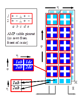
Figure 7 : JEM input map (barrel)
The serial link input signals are brought to the JEM by shielded parallel pair cable assemblies. The cables are high density halogen free 4-pair cable assemblies, of type AMP (TYCO) 1370754-1. The cable assembly is designed to connect to standard 2mm PCI style backplane connectors. The signals are passed through the backplane and received on the JEM rear edge connector. For pinout see sect. 4.2. The mapping of PPM[12] channels to JEMs is shown in Figure 7 (for FCAL JEM map see 3.5; cable numbers are shown in Table 5). Note that the V-bin channels (bottom connector) are mapped onto the cable differently so as to allow a row of the ground pins on connector row c between the LVDS signals and adjacent FIO lines (sect. 4.2).
The grounds of all serial cable assemblies entering each crate are connected to a common chassis ground on the backplane. A connection to the signal ground will be made in the back of the crate at the ground bar. The chassis ground is fed into the JEMs on the cable ground pins. According to the common grounding scheme of the JEP and the CP there will be no low impedance connection between signal ground and chassis ground anywhere on the JEM (though this would be possible via links, if required).
The LVDS signal pairs are routed via 100W differential micro strip lines on the top and bottom layers of the JEM. They are fed into the input daughter modules via 100R differential connectors (SAMTEC). On the input modules the differential lines are terminated with a single resistor near the LVDS deserialisers. The deserialisers are supplied with separate analogue and digital +3.3V supply voltages. The analogue (and PLL supply) and the digital supply voltages are routed on power planes, with all of the devices connected to the two planes. The analogue power plane is supplied from the 3.3V backplane power connector. On the JEM the deserialiser device SCAN921260 is used. It is compatible to the serialisers used on the PPM. It has been tested thoroughly with various LVDS signal sources (DSS, LSM), including a PPM carrying the final pre-compensation circuitry. The deserialisers are supplied with a reference clock (CLKDES1), which is distributed via the input processors.
The LVDS link output signals are fed into the input processor FPGA. Each input processor handles 12 electromagnetic and 12 hadronic links corresponding to three j-bins of trigger space. Each of the channels is composed of a data strobe and 10 data bits (9 bit energy + odd parity). An additional /LOCK signal flags link errors. All signals are run on tracks of only a few cm of length.
3.2 Jet input data conditioning
Data read out from the deserialiser chips are clocked into input flip-flops (IFD) on the input processor FPGAs. The use of input flip-flops guarantees predictable board level timing. The data have an arbitrary phase offset to the system clock and need to be synchronised.
Due to device and cable skew all serial data links operate on different phases. It is assumed that the pre-processors run at a skew of only a couple of nanoseconds, and the JEM bunch clock signals will be deskewed in the TTCrx to an accuracy of the order of ns. Cable length tolerances will be +/- 5 cm. From the link chip set data sheet, we expect a maximum skew of 7ns. This suggests that the combined effects of clock skew and jitter will be well below one bunch clock tick. A mechanism for correction of sampling phase and per-channel latency will, however, be provided on the JEM. On the prototype JEMs a firmware based phase detection was used. This, however, does not at the same time determine the channel-to-channel skew in terms of full ticks. Therefore a separate software-based measurement of the skew was required.
Currently a fully software-driven method for determination of optimum input sampling phases using fine grain delay scans is being developed. The de-serialised data are latched into input flip-flops concurrently on two clock phases (0°, 180°), derived from the global bunch clock. Due to the large width of the data window (almost a full period of the 40MHz clock) either of the two data samples is guaranteed to be latched in error-free. Under VME control the error-free sample is selected and routed to the algorithms. Correction of larger channel-to-channel skew in terms of full bunch ticks is done via programmable length shift registers. At start of run the information required to select the proper sample is taken from a database. The database is filled during calibration runs required after any module swapping or re-cabling.
A calibration run cycles binary counter patterns (linear ramp) in the PPr playback memories. All PPr channels are generating the ramps in phase. On the JEMs the data are read into spy memories and read out via VME. Only the first few samples of the spy data are required. In a delay scan these samples are taken for 24 different clock phase settings (TTCrx controlled), spaced 1.04 ns. Thus for each of the 24 samples the data value of two consecutive data words is recorded. Most likely the delay scan will for one or several delay values read in data that are not valid, since they are changing near the clock edge and violate setup or hold times. However, this information is not required to determine the optimum phase selection. The point in time where the data change between two consecutive ticks is recorded, as well as the absolute data values. Therefore all information needed to calculate phase and coarse delay setting is available and software can be employed to calculate the actual data base entries.
The synchronisation stage covers only the 10 data bits. The link error information (/LOCK) is latched into a single flip-flop on the rising edge of the bunch clock. Once all input signals are in phase with the global clock, they are copied to the slice readout circuitry (see sect.3.6). In the real-time data path the parity of 9 data bits is checked against the odd parity bit transmitted along with the data. The data
bits are zeroed if a parity error occurs, or upon a loss of lock. Parity errors are counted in saturating 12-bit counters. A loss of lock count is determined from the leading edge of the /LOCK signal. 12-bit saturating counters are used for this purpose. The lock loss count information is complemented by the current link status information which is read into VME along with the counter information. The error counters are reset via VME. Faulty channels can be zeroed under VME control via mask bit in the channel control register.
Jet elements are built by adding corresponding electromagnetic and hadronic energies. The summation yields a 10-bit energy. Throughout the JEP, overflows are indicated by saturation of the data field to its largest binary representation. Therefore a value of 0x1FF in either an electromagnetic or hadronic channel will saturate the jet element to 0x3FF.
The jet elements are multiplexed to a 5-bit wide word at twice the bunch clock rate, with the least significant bits sent first. The data are driven to board level via output flip-flops clocked at twice the bunch clock rate. All four jet elements per φ-bin are sent to the jet processor, while copies of three of the data words (the two leftmost elements to the JEM on the left (-h), the rightmost element to the JEM on the right) are sent across the backplane to adjacent modules.
Calculation of EX and EY is performed with hardware multipliers available in Virtex-2 FPGAs. The coefficients are VME-programmable. Therefore FCAL channels (sect 3.5) do not require any special handling as far as energy summation is concerned. Pre-summed jet elements (scalar and vector sums) are forwarded to the sum processor.
3.3
Jet
processing
The jet algorithm is performed in the jet processor FPGA, which receives up to 77 jet elements. A series of interconnected adder trees produces 60 sums of 2x2 jet elements, which are compared with next neighbours to identify local maxima. In parallel with the local maximum identification, 3x3 and 4x4 sums of jet elements are also produced. For each 2x2 subregion of the JEM’s 4x8 central jet elements, an appropriate ROI position is determined, and 2x2, 3x3, and 4x4 cluster sums associated with that position are compared with threshold energies. Eight sets of jet cluster size and energy threshold criteria can be programmed via VME for the central jets, as well as four sets for FCAL jets. If desired, the capability to have two different sets of threshold definitions in a JEM for different h-slices may be added in the future. In the case of 2x2 or 4x4 clusters tested against a threshold, only one cluster is associated with any ROI, and therefore only one comparison is necessary. For 3x3 clusters, an ROI position is associated with four clusters. In this case, the jet cluster criterion is met if at least one of these clusters exceeds the threshold.
JEMs covering FCAL regions have two sets of jet cluster criteria. If the 2x2 cluster, associated to the local maximum, contains an FCAL element, the 4 FCAL jet criteria are tested. Otherwise the 8 central jet criteria are tested. No subregion can contain both a central and an FCAL jet simultaneously.
Clusters with saturated jet elements (value 0x3FF) are automatically flagged as saturated. Setting the thresholds to full scale (0x3FF) will suppress hit and ROI data.
For central JEMs, eight 3-bit jet
multiplicities are produced for transmission to the CMM. If a jet multiplicity
exceeds
For each 2x2 subregion, the 2-bit ROI position is sent to the buffer for ROI readout, as well as 8 bits corresponding to the different threshold criteria passed and one saturation bit. The ROIs are reported in four bit streams, two with information from central ROIs and two containing FCAL ROI information. Both streams have identical formats, including 8 threshold bits (even though only 4 are reported for FCAL on the backplane and DAQ-stream).
3.4
Energy
sum processing
The sum processor receives 40 bits of energy information from each of the input processors R, S, T. Nominally 25ns wide data windows on the incoming data are guaranteed by the use of input flip-flops on the data lines. The input clock is derived from the bunch clock in an on-chip DLL. Due to the low skew on the data paths into the sum processor and the low data rate, all signals can be latched on a common clock edge.
The total transverse energy path consists of a 3-input adder with 12 bit wide inputs only. The missing energy path consists of a pair of 3-input adders for the pre-sums of the x- and y-projections of the transverse energies. Incoming data are 14-bit wide at a scale of 0.25GeV/bit. After summation the two least significant bits are stripped off.
Overflows in the energy summation trees are saturated to 12-bit full scale (4095 GeV). Saturated input channels enforce a 12-bit saturation, as well. The 12-bit energy data are each encoded to a 8-bit word with parity. It will be possible to implement the encoding and parity generation in a single-step lookup table if it is found to be beneficial with respect to latency. This implementation will allow for an arbitrary transfer function to be used in the encoder. The present implementation is, however, based on CLB resources and uses a fixed quad-linear code. Dependent on the magnitude the incoming 12-bit number is divided by a scale factor (Table 2). The resulting 6-bit word is prepended with 2 scale bits.
|
Range |
Scale
Factor |
Scale bits |
|
0-63 |
1 |
00 |
|
64-255 |
4 |
01 |
|
256-1023 |
16 |
10 |
|
1024-4095 |
64 |
11 |
Table 2 : scales
The energy sums are encoded to a single 24-bit word plus an odd parity bit. Both the jet and energy results are latched on output flip-flops at the bunch clock rate, and driven directly down the backplane at 2.5V signal level. The signals are DCI source-terminated to the line impedance of 60 Ohms.
3.5
FCAL
and endcap calorimeter treatment
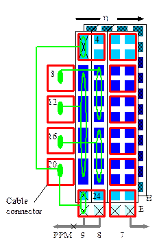
Figure 8 : FCAL map (JEM 0)
In each quadrant the left hand and right hand JEMs (JEMs 0,7,8,15) process endcap and FCAL signals (from PPMs 8 and 9) on their two outermost h-bins. While barrel JEMs are fed with cables that cover 2´2 bins in the j´h trigger space, those two h-bins are fed with cables carrying a single h bin only. The FCAL signals correspond to a double-width bin in j, so a single 4-channel cable covers a full j-quadrant.
To process the FCAL and endcap channels together with jet elements in the barrel, these channels must be rearranged in the jet processor. Double-width j bins are divided equally over two neighbouring jet elements. To that end the jet processor bit-shifts FCAL signals and copies them to the neighbouring channel in j, which is not connected to an external signal on FCAL JEMs. FCAL and endcap signals are routed to their proper locations. Re-routing of the signals is achieved by multiplexers. They are controlled by VME register bits on the jet processor. No special treatment is required on the energy sum tree, since the multiplier coefficients are controlled by software. Figure 8 shows the cabling for JEM0, the FCAL JEM at negative h. The cable numbers[13] corresponding to low h are re-mapped. For +h FCAL JEMs the cable numbers corresponding to high eta are re-mapped (see Table 5).
The use of FCAL signals (cable12) [14] allows for an energy trigger space of |h| < 4.9. Cables 4 and 24 carry endcap fanout signals required by the jet algorithm. An extension of the jet algorithm up to |h| < 4.9 requires FCAL signal fanout (cable 20). Since the jet elements are rearranged as described above, there is no special forward trigger code required in the jet processor. Special forward trigger algorithms different from the barrel code are possible only within the limits of FPGA resources and connectivity on the real-time data path. On the merger links the data bit count is limited to 25, including parity.
3.6
DAQ
and RoI
The JEM readout to DAQ and Level-2 is handled by two functionally identical logic blocks, the Read Out Controllers (ROCs), located on both the sum and jet processor. The ROC controls and reads out local readout sequencers (R/S) located in the processor FPGAs. An additional R/S implemented along with each ROC captures and pipelines bunch crossing information for local readout. Since all readout FIFOs on the JEM are the same depth, the ROC can determine FIFO fill status locally for monitoring by VME if required.
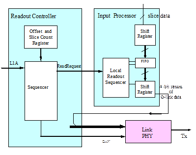
Figure 9 : Overview of the read-out logic.
The control logic for the Input FPGA readout is shown in Figure 9. DAQ read-out of the sum processor FPGAs is performed similarly. The sum processor is fed with parallel DAQ data by the jet processor and serialises the jet count information as shown above. The RoI read-out follows the same principles, with the exception that only one time slice is read out for each L1A. For efficient resource use, the latency pipeline is implemented using SelectRAM 16-bit shift registers. Total shift register depth is selected in the FPGA configuration file and cannot be modified at runtime. Therefore, the shift register depth must be tailored to cover the maximum possible downstream latency. Differences in readout latency for the various sampling points in the jet / energy algorithm are taken into account in the design of the buffers. Correct timing of the readout is therefore guaranteed by design rather than by adjustment[15]. A VME-programmable register in the ROC sets the delay of the ReadRequest signal, which initiates the transfers of data at the end of the pipeline into the 256 slice deep FIFO. To read out n slices per BC the ReqRead signal is cycled n times.
Under the control of the local Read-Out Sequencer (R/S) logic on the processor FPGAs, data are moved from the end of the latency pipeline to the derandomiser FIFO, built from block memory (18Kbit). When the derandomiser buffer is not empty, serial readout is initiated through the FIFO read port. The sum processor FPGA uses two block memories in parallel for DAQ readout, while the Input FPGAs each use 9. The parallel data streams from the FIFOs are serialized to single-bit streams by a shift register. An odd parity bit is generated and appended to the end of the resulting bit stream. The R/S concatenates all of the slices from each event into one large packet. Data from different events are separated by at least one bit of invalid data. Slice data from the processor FPGAs are appended with fill bits to make their bit streams the same length as the Input FPGA data packets.
The input processor data streams and the sum processor bit stream are forwarded to the DAQ link chip, along with further data generated within the ROC, containing the BC number. The BC number is generated by a local counter driven by the 40 MHz system clock, and reset by a derivative of the TTCRx BcntRes strobe. For multi-slice readout the BC number must be latched to ensure that all slices are tagged with the same BC number corresponding to the triggered event. The readout of Jet RoIs is carried out in a similar manner.
The assembled readout data words are synchronised to crystal clock. The baseline is 40 MHz operation. A later upgrade will be possible within the limitations of the receiving ROD. The use of a local crystal clock is mandatory due to the unknown jitter figures for the recovered LHC bunch clock. Unused data bits are forced to ground. Data are sent along with a strobe to the link PHY chips. AGILENT HDMP-1032, a device compatible to the HDMP-1022 / HDMP-1024 chip set will be used. The device operates in 16-bit mode only and uses the encoding[16] imposed by the receiving device located on the ROD. HDMP-1032 has been thoroughly tested with both the 6U Prototype RODs and 9U RODs. The serial outputs of the link chips are routed differentially to the transmitter lines of SFP sockets, which can be loaded with any commercial opto-transceiver capable of 1Gb/s data rate or higher. Both the link chips and the opto transceivers are mounted on the readout module (RM). There is no need to switch off the transmitters for reason of eye safety, though the tracking is available to add this functionality through a firmware upgrade at a later stage.
3.6.1
DAQ
read-out
A single
slice of DAQ data is 67 bits in length, including an appended odd parity bit
(see sect. 4). Up to 5 slices are read out for each L1A during
data taking. The number of slices to be read out is under the control of the
ROC, and determined by a VME-accessible register. For multi-slice read-out, the
ROC generates a correctly timed sequence of (consecutive) ReadReq
commands and passes the incoming slice data to the link chip. Since the bunch
crossing number information is unavailable to the local pipeline and readout
logic, the correct selection of slices depends on proper timing of the ReadReq signal in conjunction with the fixed-latency
pipeline.
3.6.2
ROI
read-out
A single
slice of ROI data is 11 bits in length per ROI (see sect. 4). Only one slice is read
out per event. All eight ROIs per JEM are serialised into a two-bit wide data
stream of 45 bits of total length, including an odd parity bit per stream. As
for the DAQ readout, the ROC passes the incoming ROI data along with the bunch
crossing number to the link chip. For FCAL JEMs another two bits serial stream
is required, transmitted on bit positions 3 and 4. These bits are forced to 0
on all other JEMs
3.7
Diagnostics
and control
3.7.1
Playback
and spy
Playback and spy memory is available on the JEM. The memory is organized in 256 slices deep dual-port RAM blocks. The playback buffers are filled through a single VME data port. Spy memories are read through a single port. Buffer memory addresses are incremented automatically upon VME write or read operation. A control register bit allows for a reset of the address counter. The address pointer to the real-time port of the RAM block is cycled when the processor is in either playback or spy mode. The mode is set by a VME command. Upon reception of a short broadcast command from the TTC the pointers of all playback and spy memories are aligned to 0. Playback memories are available on the input processors only. Their data are injected into the real-time data path just after the input synchronisation stage. Spy memories capture data at both the output of the synchronisation stage of the input processors and on the outputs of the jet and sum processors. Additionally the jet processor allows for readout of all input data.
3.7.2
VME
control
The VME-- interface implements a subset of standard VME-64 signals and commands. It allows for D16/A24 access to the JEM. 3.3V-CMOS bus transceivers are used. To improve testability boundary scannable devices have been chosen. Basic VME access is implemented in a CPLD located on the control daughter module (CM, Figure 1). The CPLD reads the geographic address lines of the JEM to determine the VME address range. The CPLD guarantees that any access to the module’s address space is terminated with a /DTACK signal. Data and addresses are fed into the sum processor. All other processors are controlled via the sum processor. The control port is operated synchronous with the bunch clock rate.
3.7.3
DCS
interface
Environmental conditions of the JEM are monitored by an on-board CAN node. It accurately measures supply voltages and board temperatures through SMBus devices and forwards the data to DCS via a 2-pin CAN link. The CAN PHY is mounted on the main board, so as to keep stubs as short as possible. The CAN microcontroller is located on the control module CM (see Figure 1). It interfaces to the main board with CAN, SMBus and the RS232 programming lines only. The CAN circuitry conforms to the L1Calo unified design, which aims at common software for all modules requiring CAN connectivity. Preparation of a common document is under way.
3.7.4
JTAG
JTAG boundary scan access is implemented in 5 separate daisy chains connecting up CPLDs, FPGAs, LVDS deserialiser, TTC and G-link modules, and buffer chips (VME). JTAG will be used for connectivity tests after module assembly. To this end the 5 chains will be joined via a front panel connector. CPLDs will be flashed through their JTAG chain. The FPGA chain is connected to a System ACE configurator.
3.7.5
FPGA
configuration
FPGAs are RAM-based programmable logic circuits that need to be configured after power-up. The default configuration method is via System ACE, a commercial product based on standard compact-flash memories. A XCCACE chip and a compact flash socket are located on the JEM main board. All FPGAs and the ACE are linked to a JTAG chain via the control module CM, where the JTAG signals are buffered and fanned out. Buffers and source termination on the TCK line are required, as experience with JEM1.0 has shown.
Flash cards written on a PC will be inserted into the CF socket and will automatically configure the JEM on power-up with a default set of configurations. An alternative configuration can be loaded from the flash card upon a request via VME. The ACE circuit is wired such that a slot-specific configuration can be loaded into the FPGAs, should this be required. Up to 8 different configurations can be handled by the ACE circuit. It takes the configurator about 6 seconds to configure all FPGAs. The hardware and firmware allow for in-situ programming of the flash memory cards via VME. The software for that, to be used on the JEM, the CMM and the ROD, is, however, not yet available.
For debug purposes the configurations can be loaded into the FPGAs directly from VME. This route bypasses the flash memories and makes use of slave parallel or serial configuration via the FPGA DIN ports.
3.7.6
Timing
System timing is based on the low skew, low jitter clock and data distribution by the TTC system. Each JEM has its own TTCrx chip mounted on a TTCDec daughter module and can derive all required board level timing signals from the two deskewed bunch clock signals and accompanying command and data words. The TTC signal arriving from the backplane on a differential pair is terminated and buffered close to the backplane connector. It is driven differentially to the TTCDec module.
The clock signal Clk40Des1 is fanned out at board level via source terminated single ended lines with a low skew buffer, closing the loop of a PLL mounted on the TTCDec. Clk40Des2 is fed directly to the jet processor. The Clk40 signal line is not tracked on the JEM. Since the TTCDec is operating as a crystal clock in case of a failure of the TTC system, no additional backup clock is required on the processors. This automatic failover mode will be the default mode for the JEM, to avoid DLLs getting out of lock in case of a loss of TTC lock. In such a case data transmitted by the JEM (to mergers / RODs) will be meaningless since the JEM is not in synchronisation with the external components. Therefore merger outputs will be forced to 0, the readout links will be disabled.
There are no multiples of the bunch clock routed on the JEM. Twice the bunch clock frequency is required on the input and jet processors. The clocks are derived internally from the on-chip DLLs.
The JEM is expected to use only a small fraction of the data and broadcast lines on the TTCrx. L1A is used to initiate readout into DAQ and level-2 trigger. BcntRes is used to reset the bunch counter located in the ROCs. The playback and spy pointers will be reset by a short broadcast command over the TTC system. Since all TTC signal lines are fed to the sum processor there is no limitation on the use of broadcasts. However, only a subset of TTC signals is routed to the other processor FPGAs. Therefore the sum processor would have to detect broadcast commands and encode them in a suitable way before sending them to the other processors, should a larger number of broadcasts be required in future. Since the TTCrx chip jitter figures depend on the fraction of I/O pins operating, the parallel buses are disabled during normal operation. This is controlled via I2C commands to the chip.
Upon a reset signal the TTCrx chip initialises an internal register with the chip ID and the I2C base address. The parameters are read into the SubAddr and Data lines. The relevant lines are wired to the desired pattern with help of resistors according to the L1Calo TTC document (http://hepwww.ph.qmul.ac.uk/l1calo/doc/out/TTCBusy.pdf). The TTCRx I2C lines are connected to the sum processor which interfaces them to the VME subsystem. This allows for readout and control of the TTCrx parameters through a set of two VME registers. I2C control code was taken over from the CPM and adapted to the different target device (Virtex-II). The register bit allocation is identical to allow for software compatibility.
3.8
Signal
levels and supply voltages
The JEM is a mixed signal level environment. Particular consideration of signal level compatibility and system noise issues is required so as to make the system work reliably. Differential signalling is employed for the trigger input signals (LVDS, 400Mb/s), TTC input signal distribution (3.3V PECL, 160 Mb/s) and CAN (100kb/s). All differential signals are routed on differential matched impedance micro strip lines only.
Single ended signals are CMOS 5V (CAN microcontroller), 3.3V (JTAG, VME, readout links, de-serialisers, CPLDs and buffers), 2.5V (merger lines) and 1.5V (FIO, processor-to-processor). FIO signals are sensed using CMOS or HSTL thresholds. To that end an external reference voltage of 0.75V is provided to the jet processor. This voltage is generated on the module by resistive division of the operating voltage of 1.5V.
5V CAN logic levels require the use of level shifters on all signal lines, including the SMB bus. Input lines into the CAN controller are protected by series resistors.
The analogue and PLL VCC pins of the LVDS de-serialisers are supplied from the 3.3V high current connector on the rear edge of the module. The 5V high current pin directly supplies the CAN circuitry only. The supply voltages of 3.3V and below are generated from +5V by step-down regulators. A separate linear regulator supplies the operating voltage (3.3V) to the VME buffers. All FPGA supply voltages are generated such that the startup ramp on power-on is within the specifications for Virtex-II (200µs – 10ms). Datel modules with 7ms maximum ramp have been chosen. They are linked together in a chain connecting status and control lines, such that the Xilinx recommended power-up sequence is generated. This reduces inrush currents to a minimum. Maximum current at power-up has been measured to be 8 A, during configuration the current is below 5A. In full operation with stress patterns delivered to all LVDS inputs, a JEM consumes less than 9A at 5V plus 3A at 3.3V. Total power dissipation is below 60W.
3.9
Iterations
JEM1.x
The version 1.0 of the JEM was subjected to rigorous tests in the home lab, at RAL and in the CERN test beam. While the real-time data path and the readout into the DAQ and the level-2 data paths have been shown to run error-free, a few issues were found in the control circuitry. The VME CPLD was found to be of insufficient size. This was partially to the fact that the VME configuration path needed some bit swapping due to a specification error on the configuration data bus connection of the sum FPGA. Also, the VME CPLD was seen deteriorating the crystal-generated configuration clock to an extent making it unsuitable for configuration. On the system ACE configuration path signal integrity issues were observed as well. Though all issues could be fixed on the modules it was felt the issues should be corrected for the final version. The CAN specifications had been revised meanwhile in an attempt to operate all calorimeter trigger modules with identical CAN controller firmware and thus the CAN circuitry required modifications as well.
So as to keep un-tested modifications to the delicate JEM main board to the minimum it was decided to move all affected circuitry (VME control, configurator control and CAN), which had been on the JEM1.0 main board, onto a further daughter module (CM).
JEM 1.1 was received back from the manufacturer with PCB errors on the LVDS input links. It was discovered that cross talk and noise on the FIO and merger lines were too high. The next iteration, JEM1.2 was manufactured with higher PCB signal layer count, wide spaced tracks and increased number of vias connecting the ground blades of the input daughter modules. Jet processor noise immunity was improved by adding an external reference voltage to enable the use of HSTL signalling. To that end the jet processor had to be upgraded to a 3 million gate device, which provides a larger pin count on the same footprint. FPGA battery voltage pins (Vbatt) were connected to ground, according to a Xilinx data sheet update.
Due to a design error a single FIO track was missing on JEM1.2, and therefore a new iteration JEM1.3 will have to go into production. The TTCdec mounting holes will be adapted to the new TTCdec specifications. So as to allow for improved power sequencing and controlled power shutdown and restart for the FPGAs, the VME buffers will be supplied from a separate linear regulator that keeps them operational while the FPGA power is cycled. Track separation of CAN RX/TX will be increased. Resistors will be added to the jet FPGA M lines to allow for optional serial configuration.
3.10
Daughter
module iterations
The input module (IM) initial version 1.0 has been produced in a batch of 20. During JEM tests (configuration issues on JEM1.0, noise issues on JEM1.1) several modules have been modified, and some were broken in this process due to difficulties of soldering on the modules in the lab. Currently 12 modules are fully functional. They have been successfully run on all JEM 1.x iterations.
In the course of JEM1.1 design it was decided that local voltage monitoring with help of an SMB sensor should be introduced on the input modules, should there be a need for a further iteration. A new input module version turned out to be necessary so as to improve signal ground connections (additional ground vias to connect to the ground blade) on the SAMTEC connectors in an attempt to reduce noise on the FIO lines. FPGA Vbatt will be connected to ground. The input module production version 1.1 will differ in just those three details from the previous iteration.
The control module (CM) houses FPGA configuration circuitry, basic VME circuitry, and the CAN microcontroller. Due to the fact that it took a while to develop a standard CAN design usable on all L1Calo modules, a simplified CM without any CAN circuitry had to be built to get JEM1.1 up. Now that the CAN reference design is finalised, an initial control module version 1.0 has been designed and submitted to the manufacturer.
The first G-link daughter module (RM 1.0) using HDMP1032 has been in use since November, 2004. The current version 1.1 has been in use since June, 2005. The design iteration has affected LEDs and SMB temperature sensing only. Also ground and VCC planes have been added. All versions have been successfully operated over a long period. Suspected malfunctions of the ROI G-links have been tracked down to various causes: defective G-link tester, software problems, jet processor firmware issues, and excessive wear of the daughter module connectors due to incorrect handling. The issues are understood and can be ruled out for the future. No further design iteration is planned, however, due to the fact that the volume production will go to a PCB manufacturer rather than a broker, the final modules will be referred to as RM1.2 and they will have the track widths controlled by the manufacturer so as to achieve a good impedance match.
3.11
Summary
of post-FDR design changes
The following module designs were presented to the reviewers: JEM1.1, IM1.0, RM1.1. The control module was presented as a conceptual design only. The following post-FDR design modifications have been made, for reason explained in parentheses:
JEM modifications 1.1à1.2:
- Increase PCB layer count (FIO cross talk)
- Increase FIO track spacing (FIO cross talk)
- Improve input daughter connector grounding by adding vias (FIO noise)
- Increase merger track spacing (cross talk on merger lines)
- Upgrade jet processor to XC2V3000 to use external voltage reference on FIOs (FIO noise)
- Connect Vbatt of processors to ground (change of device specifications)
JEM modifications 1.2à1.3:
- New TTCdec mounting holes (specification change)
- Add missing FIO track (design error)
- Supply VME bus buffers from separate 3.3V regulator to allow for control of the switching regulators via CAN (pre-caution to deal with non-reproducible issue of FPGAs not configuring up, seen exactly once)
- Increase CAN TX/RX track spacing (design error)
IM modifications 1.0à1.1:
- Improve ground blade conmnection (FIO noise)
- Add SMB voltage sensor
- Connect Vbatt to ground (change of device specifications)
RM modifications 1.0à1.1:
- Go for 4-layer PCB (FDR)
- Add link ready / laser on LED
RM modifications 1.1à1.2: use impedance controlled tracking
CM : initial design
4 Interfaces :
connectors, pinouts, data formats
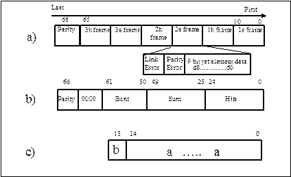
Figure 10 : 16-bit slice data bit stream format (a-b)
and readout link bit map (c)
3e/h frames zeroed on G-link bit 14
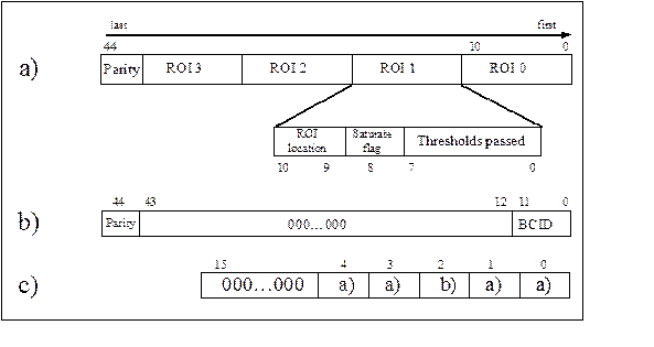
Figure 11 : RoI data bit stream format (a-b) and readout link bit map (c)
Figure 12 : RoI numbering scheme
|
LVDS de-serialiser Rout |
9 |
8 |
7 |
6 |
5 |
4 |
3 |
2 |
1 |
0 |
|
Trigger data bit |
8 |
7 |
6 |
5 |
4 |
3 |
2 |
1 |
0 |
P |
Table 3 : serial input data bits
|
SYSRESET |
1 |
|
A[23..1] |
23 |
|
D[15..0] |
16 |
|
DS0* |
1 |
|
Write* |
1 |
|
DTACK* |
1 |
|
Total Number |
43 |
Table 4 VME signals
|
|
E0, E1 |
E2, E3 |
|
H0, H1 |
H2,H3 |
|
W,X |
4 |
2 |
|
3 |
1 |
|
G,H |
8 |
6 |
|
7 |
5 |
|
E,F |
12 |
10 |
|
11 |
9 |
|
C,D |
16 |
14 |
|
15 |
13 |
|
A,B |
20 |
18 |
|
19 |
17 |
|
V |
24 |
22 |
|
23 |
21 |
Table 5 cable numbers, as seen from front of crate
|
80 |
82 |
84 |
86 |
|
72 |
74 |
76 |
78 |
|
64 |
66 |
68 |
70 |
|
56 |
58 |
60 |
62 |
|
48 |
50 |
52 |
54 |
|
40 |
42 |
44 |
46 |
|
32 |
34 |
36 |
38 |
|
24 |
26 |
28 |
30 |
|
16 |
18 |
20 |
22 |
|
8 |
10 |
12 |
14 |
|
0 |
2 |
4 |
6 |
Table 6 η/φ-map of channel numbers (electromagnetic), as seen
from front of crate
4.1
Front
panel
|
# |
Socket type |
Socket use |
|
2 |
Opto LC |
DAQ and ROI (receiver not in use) |
|
1 |
Lemo |
Deskewed-1 clock (terminate 50 R, 500mV) |
|
1 |
Sub-D 15 pin male |
JTAG |
|
1 |
Sub-D 9 pin female |
CAN controller ISP |
|
1 |
Compact flash socket |
System ACE flash card |
|
# |
LED colour |
LED use |
|
|
|
|
|
1 |
green |
Readout links ready / laser on |
|
|
|
|
|
1 |
yellow |
VME access (stretched) |
|
1 |
yellow |
L1Accept (stretched) |
|
2 |
yellow |
spare |
|
9 |
green |
VCC ok |
|
6 |
green |
FPGA configuration done (incl. control FPGA) |
|
1 |
green |
TTC ok (S1) |
|
3 |
green |
spare |
|
1 |
red |
Input link error (stretched) |
|
1 |
red |
Input parity error (stretched) |
|
2 |
red |
spare |
|
|
|
|
|
1 |
green |
System ACE active / ok |
|
1 |
red |
System ACE error |

4.2 backplane connector layout
|
Pos. |
A |
B |
C |
D |
E |
Guide Pin (0-8mm) (AMP parts 223956-1, 223957-1, or equivalent)
Connector 1 (8-58mm) Type B-25 connector (short through-pins)
|
1 |
SMM0 |
<G> |
VMED00 |
VMED08 |
VMED09 |
|
2 |
SMM1 |
VMED01 |
VMED02 |
VMED10 |
VMED11 |
|
3 |
SMM2 |
<G> |
VMED03 |
VMED12 |
VMED13 |
|
4 |
SMM3 |
VMED04 |
VMED05 |
VMED14 |
VMED15 |
|
5 |
SMM4 |
<G> |
VMED06 |
VMEA23 |
VMEA22 |
|
6 |
SMM5 |
VMED07 |
<G> |
VMEA21 |
VMEA20 |
|
7 |
SMM6 |
<G> |
VMEDS0* |
<G> |
<G> |
|
8 |
SMM7 |
VMEWRITE* |
<G> |
VMEA18 |
VMEA19 |
|
9 |
SMM8 |
<G> |
VMEDTACK* |
VMEA16 |
VMEA17 |
|
10 |
SMM9 |
VMEA07 |
VMEA06 |
VMEA14 |
VMEA15 |
|
11 |
SMM10 |
<G> |
VMEA05 |
VMEA12 |
VMEA13 |
|
12 |
SMM11 |
VMEA04 |
VMEA03 |
VMEA10 |
VMEA11 |
|
13 |
SMM12 |
<G> |
VMEA02 |
VMEA08 |
VMEA09 |
|
14 |
SMM13 |
VMERESET* |
VMEA01 |
<G> |
<G> |
|
15 |
SMM14 |
<G> |
<G> |
FL0 |
FR0 |
|
16 |
SMM15 |
FL1 |
FL2 |
<G> |
FR1 |
|
17 |
SMM16 |
<G> |
FL3 |
FR2 |
FR3 |
|
18 |
SMM17 |
FL4 |
FL5 |
<G> |
FR4 |
|
19 |
SMM18 |
<G> |
FL6 |
FR5 |
FR6 |
|
20 |
SMM19 |
FL7 |
FL8 |
<G> |
FR7 |
|
21 |
SMM20 |
<G> |
FL9 |
FR8 |
FR9 |
|
22 |
SMM21 |
FL10 |
FL11 |
<G> |
FR10 |
|
23 |
SMM22 |
<G> |
FL12 |
FR11 |
FR12 |
|
24 |
SMM23 |
FL13 |
FL14 |
<G> |
FR13 |
|
25 |
SMM24 |
<G> |
FL15 |
FR14 |
FR15 |
Connector 2
(58-96mm) Type
B-19 connector (mixed short/long through pins)
|
1 |
FL16 |
FL17 |
FR16 |
<G> |
FR17 |
|
2 |
FL18 |
<G> |
FL19 |
FR18 |
FR19 |
|
3 |
FL20 |
FL21 |
FR20 |
<G> |
FR21 |
|
4 |
FL22 |
<G> |
FL23 |
FR22 |
FR23 |
|
5 |
FL24 |
FL25 |
FR24 |
<G> |
FR25 |
|
6 |
FL26 |
<G> |
FL27 |
FR26 |
FR27 |
|
7 |
FL28 |
FL29 |
FR28 |
<G> |
FR29 |
|
8 |
FL30 |
<G> |
FL31 |
FR30 |
FR31 |
|
9 |
FL32 |
FL33 |
FR32 |
<G> |
FR33 |
|
10 |
GEOADD5 |
<G> |
GEOADD4 |
<G> |
GEOADD3 |
|
11 |
1+ Cable 1 |
1- |
<SG> |
2+ |
2- |
|
12 |
3+ |
3- |
<SG> |
4+ |
4- |
|
13 |
1+ Cable 2 |
1- |
<SG> |
2+ |
2- |
|
14 |
3+ |
3- |
<SG> |
4+ |
4- |
|
15 |
1+ Cable 3 |
1- |
<SG> |
2+ |
2- |
|
16 |
3+ |
3- |
<SG> |
4+ |
4- |
|
17 |
1+ Cable 4 |
1- |
<SG> |
2+ |
2- |
|
18 |
3+ |
3- |
<SG> |
4+ |
4- |
|
19 |
GEOADD2 |
<G> |
GEOADD1 |
<G> |
GEOADD0 |
Connector 3
(96-134mm) Type B-19 connector (mixed short/long through pins)
|
1 |
FL34 |
FL35 |
FR34 |
<G> |
FR35 |
|
2 |
FL36 |
<G> |
FL37 |
FR36 |
FR37 |
|
3 |
FL38 |
FL39 |
FR38 |
<G> |
FR39 |
|
4 |
FL40 |
<G> |
FL41 |
FR40 |
FR41 |
|
5 |
FL42 |
FL43 |
FR42 |
<G> |
FR43 |
|
6 |
FL44 |
<G> |
FL45 |
FR44 |
FR45 |
|
7 |
FL46 |
FL47 |
FR46 |
<G> |
FR47 |
|
8 |
FL48 |
<G> |
FL49 |
FR48 |
FR49 |
|
9 |
FL50 |
FL51 |
FR50 |
<G> |
FR51 |
|
10 |
<G> |
<G> |
<G> |
<G> |
<G> |
|
11 |
1+ Cable 5 |
1- |
<SG> |
2+ |
2- |
|
12 |
3+ |
3- |
<SG> |
4+ |
4- |
|
13 |
1+ Cable 6 |
1- |
<SG> |
2+ |
2- |
|
14 |
3+ |
3- |
<SG> |
4+ |
4- |
|
15 |
1+ Cable 7 |
1- |
<SG> |
2+ |
2- |
|
16 |
3+ |
3- |
<SG> |
4+ |
4- |
|
17 |
1+ Cable 8 |
1- |
<SG> |
2+ |
2- |
|
18 |
3+ |
3- |
<SG> |
4+ |
4- |
|
19 |
<G> |
<G> |
<G> |
<G> |
<G> |
Connector 4 (134-172mm) Type B-19 connector (short through pins)
|
1 |
FL52 |
FL53 |
FR52 |
<G> |
FR53 |
|
2 |
FL54 |
<G> |
FL55 |
FR54 |
FR55 |
|
3 |
FL56 |
FL57 |
FR56 |
<G> |
FR57 |
|
4 |
FL58 |
<G> |
FL59 |
FR58 |
FR59 |
|
5 |
FL60 |
FL61 |
FR60 |
<G> |
FR61 |
|
6 |
FL62 |
<G> |
FL63 |
FR62 |
FR63 |
|
7 |
FL64 |
FL65 |
FR64 |
<G> |
FR65 |
|
8 |
FL66 |
<G> |
FL67 |
FR66 |
FR67 |
|
9 |
FL68 |
FL69 |
FR68 |
<G> |
FR69 |
|
10 |
<G> |
<G> |
<G> |
<G> |
<G> |
|
11 |
1+ Cable 9 |
1- |
<SG> |
2+ |
2- |
|
12 |
3+ |
3- |
<SG> |
4+ |
4- |
|
13 |
1+ Cable 10 |
1- |
<SG> |
2+ |
2- |
|
14 |
3+ |
3- |
<SG> |
4+ |
4- |
|
15 |
1+ Cable 11 |
1- |
<SG> |
2+ |
2- |
|
16 |
3+ |
3- |
<SG> |
4+ |
4- |
|
17 |
1+ Cable 12 |
1- |
<SG> |
2+ |
2- |
|
18 |
3+ |
3- |
<SG> |
4+ |
4- |
|
19 |
<G> |
<G> |
<G> |
<G> |
<G> |
Connector 5
(172-210mm) Type B-19 connector (mixed short/long through pins)
|
1 |
FL70 |
FL71 |
FR70 |
<G> |
FR71 |
|
2 |
FL72 |
<G> |
FL73 |
FR72 |
FR73 |
|
3 |
FL74 |
FL75 |
FR74 |
<G> |
FR75 |
|
4 |
FL76 |
<G> |
FL77 |
FR76 |
FR77 |
|
5 |
FL78 |
FL79 |
FR78 |
<G> |
FR79 |
|
6 |
FL80 |
<G> |
FL81 |
FR80 |
FR81 |
|
7 |
FL82 |
FL83 |
FR82 |
<G> |
FR83 |
|
8 |
FL84 |
<G> |
FL85 |
FR84 |
FR85 |
|
9 |
FL86 |
FL87 |
FR86 |
<G> |
FR87 |
|
10 |
<G> |
<G> |
<G> |
<G> |
<G> |
|
11 |
1+ Cable 13 |
1- |
<SG> |
2+ |
2- |
|
12 |
3+ |
3- |
<SG> |
4+ |
4- |
|
13 |
1+ Cable 14 |
1- |
<SG> |
2+ |
2- |
|
14 |
3+ |
3- |
<SG> |
4+ |
4- |
|
15 |
1+ Cable 15 |
1- |
<SG> |
2+ |
2- |
|
16 |
3+ |
3- |
<SG> |
4+ |
4- |
|
17 |
1+ Cable 16 |
1- |
<SG> |
2+ |
2- |
|
18 |
3+ |
3- |
<SG> |
4+ |
4- |
|
19 |
<G> |
<G> |
<G> |
<G> |
<G> |
Connector 6
(210-248mm) Type B-19 connector (mixed short/long through pins)
|
1 |
FL88 |
FL89 |
FR88 |
<G> |
FR89 |
|
2 |
FL90 |
<G> |
FL91 |
FR90 |
FR91 |
|
3 |
FL92 |
FL93 |
FR92 |
<G> |
FR93 |
|
4 |
FL94 |
<G> |
FL95 |
FR94 |
FR95 |
|
5 |
FL96 |
FL97 |
FR96 |
<G> |
FR97 |
|
6 |
FL98 |
<G> |
FL99 |
FR98 |
FR99 |
|
7 |
FL100 |
FL101 |
FR100 |
<G> |
FR101 |
|
8 |
FL102 |
<G> |
FL103 |
FR102 |
FR103 |
|
9 |
FL104 |
FL105 |
FR104 |
<G> |
FR105 |
|
10 |
<G> |
<G> |
<G> |
<G> |
<G> |
|
11 |
1+ Cable 17 |
1- |
<SG> |
2+ |
2- |
|
12 |
3+ |
3- |
<SG> |
4+ |
4- |
|
13 |
1+ Cable 18 |
1- |
<SG> |
2+ |
2- |
|
14 |
3+ |
3- |
<SG> |
4+ |
4- |
|
15 |
1+ Cable 19 |
1- |
<SG> |
2+ |
2- |
|
16 |
3+ |
3- |
<SG> |
4+ |
4- |
|
17 |
1+ Cable 20 |
1- |
<SG> |
2+ |
2- |
|
18 |
3+ |
3- |
<SG> |
4+ |
4- |
|
19 |
<G> |
<G> |
<G> |
<G> |
<G> |
Connector 7
(248-286mm) Type B-19 connector (mixed short/long through pins)
|
1 |
FL106 |
FL107 |
FR106 |
<G> |
FR107 |
|
2 |
FL108 |
<G> |
FL109 |
FR108 |
FR109 |
|
3 |
FL110 |
FL111 |
FR110 |
<G> |
FR111 |
|
4 |
FL112 |
<G> |
FL113 |
FR112 |
FR113 |
|
5 |
FL114 |
FL115 |
FR114 |
<G> |
FR115 |
|
6 |
FL116 |
<G> |
FL117 |
FR116 |
FR117 |
|
7 |
FL118 |
FL119 |
FR118 |
<G> |
FR119 |
|
8 |
FL120 |
<G> |
FL121 |
FR120 |
FR121 |
|
9 |
FL122 |
FL123 |
FR122 |
<G> |
FR123 |
|
10 |
<G> |
<G> |
<G> |
FL124 |
FR124 |
|
11 |
1+ Cable 21 |
1- |
<SG> |
<G> |
FR125 |
|
12 |
3+ |
3- |
<SG> |
FL125 |
FL126 |
|
13 |
1+ Cable 22 |
1- |
<SG> |
<G> |
FR126 |
|
14 |
3+ |
3- |
<SG> |
FL127 |
FR127 |
|
15 |
1+ Cable 23 |
1- |
<SG> |
<G> |
FR128 |
|
16 |
3+ |
3- |
<SG> |
FL128 |
FL129 |
|
17 |
1+ Cable 24 |
1- |
<SG> |
<G> |
FR129 |
|
18 |
3+ |
3- |
<SG> |
FL130 |
FR130 |
|
19 |
<G> |
<G> |
<G> |
FL131 |
FR131 |
Connector 8 (286-336mm) Type B-25 connector (short through pins)
|
1 |
FL132 |
FR132 |
FR133 |
<G> |
JMM0 |
|
2 |
FL133 |
<G> |
FL134 |
FR134 |
JMM1 |
|
3 |
FL135 |
FR135 |
FR136 |
<G> |
JMM2 |
|
4 |
FL136 |
<G> |
FL137 |
FR137 |
JMM3 |
|
5 |
FL138 |
FR138 |
FR139 |
<G> |
JMM4 |
|
6 |
FL139 |
<G> |
FL140 |
FR140 |
JMM5 |
|
7 |
FL141 |
FR141 |
FR142 |
<G> |
JMM6 |
|
8 |
FL142 |
<G> |
FL143 |
FR143 |
JMM7 |
|
9 |
FL144 |
FR144 |
FR145 |
<G> |
JMM8 |
|
10 |
FL145 |
<G> |
FL146 |
FR146 |
JMM9 |
|
11 |
FL147 |
FR147 |
FR148 |
<G> |
JMM10 |
|
12 |
FL148 |
<G> |
FL149 |
FR149 |
JMM11 |
|
13 |
FL150 |
FR150 |
FR151 |
<G> |
JMM12 |
|
14 |
FL151 |
<G> |
FL152 |
FR152 |
JMM13 |
|
15 |
FL153 |
FR153 |
FR154 |
<G> |
JMM14 |
|
16 |
FL154 |
<G> |
FL155 |
FR155 |
JMM15 |
|
17 |
FL156 |
FR156 |
FR157 |
<G> |
JMM16 |
|
18 |
FL157 |
<G> |
FL158 |
FR158 |
JMM17 |
|
19 |
FL159 |
FR159 |
FR160 |
<G> |
JMM18 |
|
20 |
FL160 |
<G> |
FL161 |
FR161 |
JMM19 |
|
21 |
FL162 |
FR162 |
FR163 |
<G> |
JMM20 |
|
22 |
FL163 |
<G> |
FL164 |
FR164 |
JMM21 |
|
23 |
<G> |
<G> |
<G> |
<G> |
JMM22 |
|
24 |
CAN+ |
<G> |
TTC+ |
<G> |
JMM23 |
|
25 |
CAN- |
<G> |
TTC- |
<G> |
JMM24 |
Connector 9 (336-361mm) Type D (N) connector
|
2 |
+3.3V |
|
6 |
Power GND |
|
10 |
+5.0V |
5 Glossary
The following lists some of the terms and acronyms used in the text.
|
CM |
Control module |
|
CMM |
Common Merger Module |
|
CP |
Cluster Processor sub-system of the Calorimeter Trigger 17 |
|
CPLD |
Complex Programmable Logic Device |
|
CPM |
Cluster Processor Module 17 |
|
CTP |
Central Trigger Processor |
|
DCS |
Detector Control System |
|
DLL |
Delay-Locked
|
|
D-ROD |
ROD with JEP DAQ firmware |
|
DSS |
Data source / sink module 17 |
|
FIO |
Fan in / fan out signal lines on the backplane |
|
FPGA |
Field Programmable Gate Array |
|
G-link |
Agilent Gigabit serial link |
|
IM |
Input module |
|
JEM |
Jet/Energy processor module |
|
JEP |
Jet/Energy Processor sub-system of the Calorimeter Trigger |
|
JEP crate |
Electronics crate processing two quadrants of trigger space with 16 JEMs |
|
jet element |
Electromagnetic+hadronic energy sum in a .2´.2 cell |
|
JTAG |
Joint Test Action Group |
|
L1Calo |
Level-1 calorimeter trigger |
|
LSM |
LVDS source module 17 |
|
LVDS |
Low-Voltage Differential Signalling |
|
PB, Backplane |
Multi-purpose high-speed common backplane within JEP and CP crate [17] |
|
PHY |
Physical layer interface chip (CAN PHY, G-link gigabit PHY) |
|
PPM |
Pre-Processor Module |
|
PPr |
Pre-Processor 17 |
|
R, S, T, U |
Input modules |
|
R/S |
Read-out sequencer |
|
RM |
Read-out module |
|
ROC |
Read-out Controller logic on the JEM |
|
ROD |
Read-Out Driver module (personalised with either R-ROD or D-ROD firmware) 17 |
|
ROI |
Region Of Interest |
|
R-ROD |
ROD with JEP ROI processor firmware |
|
SMB |
System management bus |
|
TCM |
Timing and Control Module 17 |
|
TTC |
Timing ,Trigger and Control |
|
TTCdec |
Timing receiver daughter module 17 |
|
TTCrx |
Timing receiver chip |
6
Figures
and tables
Figure
1: Block diagram of JEM, including daughter modules R,S,T,U, RM, CM, TTCDec
Figure
2 : JEM input processor : jet element formation, one out of 44 jet elements
shown
Figure
3 : JEM energy processing
Figure
4: RoI and DAQ slice data path
Figure
5 : Input processor : readout sequencer
Figure
7 : JEM input map (barrel)
Figure
9 : Overview of the read-out logic.
Figure
11 : RoI data bit stream format (a-b) and readout link bit map (c)
Figure
12 : RoI numbering scheme
Table 3 : serial input data
bits
Table 5 cable numbers, as
seen from front of crate
Table 6 η/φ-map of
channel numbers (electromagnetic), as seen from front of crate
Change log:
2005-12-12 add jet processor properties to table 1 (Version 1.1d)
2005-12-09 add SMB level translator and power consumption to sect. 3.8. Update 1.21, 2.5, 3.3, 3.5 (jet related issues)
2005-12-02 move test results and programming model to separate documents. Implement FDR comments except jet related issues. Add module history. Modifications to describe JEM1.3 correctly
2005-03-26 first released version relating to JEM1.0 and JEM 1.1 (V1.0)