Notes on Topology
Processor Development
2 Design principles –
do it simple
1
Development line
Original
plans were for the following sequence:
GOLD – prototype1– prototype2 – production modules – additional production
modules for 2018.
However,
adding further identical modules in 2018 might actually require additional low-latency
backplane connectivity on currently designed modules, to allow for
module-to-module data transfer. Due to limited connectivity on current FPGAs,
that might possibly compromise the chip-to-chip link capacity.
Therefore,
rather consider cutting cost on prototyping and production modules for 2013,
and be prepared to replace topo modules in 2018 (or earlier), if
module-to-module data transmission were required. That might mean another
prototype in 2015. Due to design optimisation on 2013 topo modules, that move
might be cost neutral.
Bandwidth
requirement had been estimated at time of Stockholm meeting (after correction
for 16 octants):
“Preliminary
data formats for jet and cluster processors: 96*(14*8+32) bit @40 MHz => 553Gb/s
For muon
data assume data volume comparable to current MUCTPI input: 16*13*32 bit @
40MHZ =>267Gb/s”, i.e. 820 Gb/s total. That’s under
the assumption that all 96 data bits from each CP/jet slot are fully
transmitted. No realistic muon data rate is known. Add some ε for energy
sums.
The Stockholm
presentation (June 2011) is found here:
See slide 6
for the block diagram, slide 7 for bandwidth estimate.
2
Design
principles – do it simple
The topo
processor prototype tries to get closest possible to the final production
module. While GOLD is toying with connectors and mezzanines, allowing for
maximum flexibility when testing data transmission, the prototype will be strictly
purpose-built. While the initial prototype is being developed, the GOLD will
continue to serve as a platform for on-going exploration of new technologies (opto links), and firmware development. Necessity for
prototype2 will depend on required maximum connectivity (see below).
Due to
recent concern about long high-speed lanes across connectors, PCBs, and
backplanes, the topo processor prototype will be optimised in the following
way:
The
processor module will, to the extent possible, make use of high-density optical
and optoelectronic components. Any duplication required will be done upstream. Any
electrical high-speed tracks will be routed on shortest possible links onto the
closest FPGA. The current scheme will possibly
even give up (t.b.d.) on the long-favoured scheme of
electrical duplication on the outputs of the opto-electrical
converters, since, when using highest density o/e converters, the track lengths
would most likely need to be extended, to fit fan-out chips. If a fan-out free
design were available early, that might increase pressure on the CMX to provide
ample output bandwidth, to allow a significant level of upstream duplication. Also,
the use of 10Gb/s technology might be encouraged, if a
high-speed sink is available at a short timeline.
Moreover,
early availability of a near-final topo prototype would allow for the CMX local
topo functionality to be removed from the requirements. This would simplify and
speed up CMX design, and allow for additional output connectivity for upstream
duplication.
The topo
processor sports two processor chips for real-time processing. They are
indicated A and B (largest available Virtex-7) in fig.1. With the devices
expected to be available by spring 2012 the total MGT input connectivity of the
topo processor would be 112 links, i.e. up to 0.9 Tb/s, if 10Gb/s
links are fed in. With 6.4Gb/s links the total bandwidth
amounts to 0.57Tb/s. The use of more
advanced FPGAs on a possible second prototype might boost the bandwidth by a
factor of 1.4 or even 1.7 (80, as presented in Stockholm,
or 96 links per chip).
Control
FPGA C (small Kintex-7) is mainly concerned with interfacing to the module
controller via Ethernet. The opto-electrical converters
are assumed of miniPOD type. They are all mounted mid board and are connected
to either front or back panel with octopus cables. While the preferred solution
is optical backplane connection, the mechanical properties of the blind mate
connectors have not yet been explored.
Dependent on
the results from the GOLD, either back or front panel connectors will be
chosen. The decision can be still taken once the PCB is manufactured. The FPGA interconnect
will be done with parallel differential links. There is a penalty of approx. 1
tick of latency, if both FPGAs need to be joined together this way. Almost all bandwidth
between FPGAs A and B will be made available for the real-time data path.
It is
anticipated to reserve one bank each for read and write control buses to C. Also,
some narrow, parallel port should be reserved for low latency connection to the
CTP.
It will
have to be discussed within the community, whether MGT links can actually be
used for Muon input (latency)! That used to be our baseline for a while, and we
should write the specs accordingly, but we do not yet know what other’s
baseline is. In case low latency parallel connectivity were needed, major modifications
of the scheme might be required. To provide the required parallel bandwidth, we
might have to make a U-turn and re-introduce a main processor FPGA!
For reason
of latency optimisation, either a symmetric dual processor scheme (fig.1) or a
hierarchic scheme seems adequate. The
latter will yield higher aggregate bandwidth.
![]()
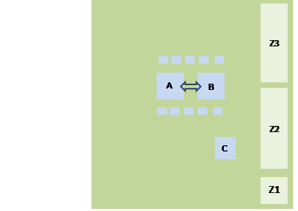
Figure 1: Floor plan topo module
It should be
noted that quite some ancillary circuitry and firmware will be required. It is anticipated
that the I2C/power control scheme can be taken over from RAL. Ethernet based control
should be adapted from Bristol and/or RAL.
3
Technicalities
Data integrity
is best preserved if minimising track length and vias on the track. Therefore the o/e converters will be mounted
close to the FPGAs. However, there is competition for real estate between o/e
converters and POL voltage converters. Vias will be avoided by optionally
connecting differential links in inverse polarity. Actual link polarity is
programmable on the FPGAs (check V7!). Consider inverse polarity option also on
parallel buses. Run MGT links on top and bottom only. If that’s ruled out for
reason of breakout density, micro or blind vias might have to be used to avoid
stubs. MGT clocks also deserve signal integrity focused attention. Check
whether clock polarity matters.
Though pin
swapping would be possible across banks, there are limitations imposed on
functionality of groups of pins. Therefore
it is decided to connect full banks of A to full banks of B. No mixing of banks.
All banks 2.5V/1.8V (check V7 specs HP/HR). LVDS only.
Due to the
required dense packing, thermal considerations are required.