Generic Optical Link Demonstrator
Introduction
The ATLAS Level-1 Calorimeter Trigger algorithms are mainly based on the analysis of localized objects (e.g. electromagnetic clusters or jets) that are identified by sliding-window algorithms. On both phase 1 and phase 2 of the trigger upgrade there will be a need for a topological post-processing of objects identified by the sliding-window processors. There are two fundamentally different approaches to processing data containing information on the event topology:
For algorithms requiring the presence of two or more objects it is sufficient to present the n most significant objects of each object type to the top level processor. Each object needs to be tagged with position, type and significance. The latter must be on a monotonous scale, such that a simple arithmetic comparison can determine the largest objects.
In hardware, this scheme maps onto a simple tree-like structure where a large number of object data is entering a processor, a sort algorithm determines the most significant ones, and a small number of objects is passed on to the final decision logic. Such architecture can easily be resolved into a large number of simple, identical stages of compare-and-select operations. The only limitation here comes from the latency induced at chip and module boundaries, in particular when high speed serial links are employed. Therefore excessive partitioning into microscopic sub-processors ought to be avoided.
For algorithms requiring the presence of one object in conjunction with the absence of another one, the scheme described above is not suitable. Here, along with each object identified, we would need the full set of data describing all sections of the solid angle that might possibly be associated with this object. In the extreme, such algorithms would require all available data to be mapped onto a single processor. Some level of data reduction might be possible, once the detailed algorithms are known. However, for a generic two-dimensional ( h , j ) topological processor, data transport into a compact and powerful processor is a major challenge.
Due to the algorithms to be used, the phase-1, as well as the phase-2 top level processors will most likely require both tree-like and two-dimensional processors. It is probably worth pointing out that for phase-2 a new sliding window processor will have to be built, which is just another two-dimensional processor as described above.
Topological
data will be carried on optical fibres. Since it will not be possible to route
all data into a single processor chip, incoming data need to be copied to
several chips, or even several modules. Data can effectively be replicated in
three different ways: electrical duplication at the source, passive fibre
couplers (splitters), and electrical duplication at the sink. Retransmission at
the sink would rather be avoided, for reason of latency.
Dependent
on the link replication scheme and on the module form factor there are various
options how to route the optical links into the module. Front panel opto
connectors are messy, once the number of links per module gets large. Rear
transition modules can be particularly useful, if links are to be replicated to
neighbouring slots electrically. However, at very high link speeds the scope
for electrical routing across backplanes and connectors is very limited. From
both logistical and signal integrity point of view the use of high-density
blind-mate optical backplane connectors is probably the most favourable
approach.
For
modules mainly based on optical connectivity, no standard form factor is known.
However, slot pitch is impractically dense for VME modules with sub-modules, in
particular when taking thermal issues into account. Also, 9Ux40cm module
dimensions are at the very limit for a densely packed, densely routed module.
Track length limitations at high speeds might force the designer to squeeze
high-speed sections of the design into just a fraction of available space.
ATCA, on the other hand, offers the advantage of a considerable backplane
height, moderate board area, and increased slot width. Rear transition modules
are integral part of the ATCA specs. Power dissipation limits on RTMs were low,
but are currently being lifted. The concept of -48V primary supply is superior
to the VME supply scheme. A combination of ATCA standard crate mechanics, ATCA
power distribution, and a custom backplane in the remaining back space would be
an attractive scheme for opto fibre based module connectivity.
It
is planned to build an ATCA sized demonstrator module, based on Xilinx Virtex-6
FPGAs and high density blind mate opto connectors. Xilinx V6 road map suggests
a time line with module manufacturing in early 2010. By then a module could be
equipped with either engineering samples or production chips. The exact dates
for availability of production silicon cannot currently be predicted. High
density blind mate opto connectors are available from a couple of companies. Currently
suitable and available products are being assessed. If the backplane optics
concept fails to convince, electro-optical RTMs would probably be preferred
over front panel connectivity.
Main
goal of the demonstrator project is the proof of concept of extensive high
speed link replication. Therefore it is planned to equip the demonstrator with
a larger number of moderately sized FPGAs. By the time a prototype will be
built, details of the algorithms will be known. Therefore one would at that
stage either convert the design to fewer large devices, so to reduce link
replication. Or, if the algorithms turn out to require large amounts of logic
resources, one would have to go for many large devices.
The
GOLD link demonstrator is a priori not dependent on any specific make of
processors or opto link components. Xilinx was chosen, since tools and
expertise are available in the labs. While the main objective is exploration of
high speed link devices and optical data transmission, the module should be
built such that it will be useful as a data sink and source module for other
modules built for of the L1Calo upgrade programme. That will lead to the implementation
of some additional interfaces not necessarily required for the bare link tester
functionality.
Requirements
The
real-time data path of the module will be via fibre optical connectors through
a backplane or an RTM. Data rate per fibre will be 6.5Gb/s. The module will
require a minimum input connectivity of 12 fibre ribbons (i.e. 144 fibres). External
connection is via 12-fibre standard MPO/MTP connectors. On the module the fibre
ribbons will have to connect into 6.5Gb/s SNAP12 receivers. Twelve of those
devices will be required. The electrical links will be duplicated in CML fan-out
devices suitable for 6.5Gb/s data rate. That requires a total of 288 FPGA-based
receivers, equivalent to a minimum of 12 FPGAs (XC6VLX240T) or 8 FPGAs (XC6VLX550T).
Currently there are no requirements known on the routing of these links. The
connectivity will have to be defined by the algorithms to be implemented.
So
as to allow for the use as a L1Calo global processor demonstrator, an
electrical interface to the CTP will be provided either at the front panel of
the module or via a backplane. In the latter case a dedicated (ATCA) backplane
would be required to route the signals to a breakout module. The signals will be
differential (LVDS).
Implementation details
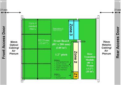
The
demonstrator will probably be built in ATCA form factor. The power supply zone
(Z1) will be compatible to a standard ATCA crate. Zone 2 will probably be
mainly unused (unless the CTP interface is made via the backplane). Board
control could possibly be done via zone 2 links. Zone 3 will carry optical link
connectors. Since all real-time backplane connectivity will be made optically,
it might make sense to run crate control, environmental, and timing data on
fibres as well. A single electrical cable connection to the CTP will probably be
made on the front panel.
|
|